

South Korea CMP Slurry Market Size & Forecast:
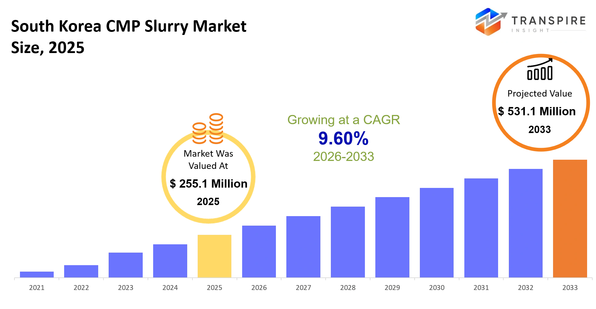
- South Korea CMP Slurry Market Size 2025: USD 255.1 Million
- South Korea CMP Slurry Market Size 2033: USD 531.1 Million
- South Korea CMP Slurry Market CAGR: 9.60%
- South Korea CMP Slurry Market Segments: By Type (Silica Slurry, Alumina Slurry, Ceria Slurry, Diamond Slurry, Others) | By Application (Semiconductors, MEMS, Optical Components, Data Storage, Others) | By Material (Copper CMP, Tungsten CMP, STI CMP, Dielectric CMP, Others) | By End User (Foundries, IDMs, OSAT Companies, Others)
South Korea CMP Slurry Market Summary
The South Korea CMP Slurry Market was valued at USD 255.1 Million in 2025. It is forecast to reach USD 531.1 Million by 2033. That is a CAGR of 9.60% over the period.
South Korea’s CMP ( Chemical Mechanical Planarization ) slurry market really matters for semiconductor making , because it lets chipmakers produce those ultra-flat wafer faces needed for advanced integrated circuits. Basically, CMP slurries remove tiny bumps and uneven bits that otherwise mess with transistor behavior, yield levels and long term device trust. As South Korea pushes harder in memory chips plus newer logic production, slurry performance is now kinda linked directly to manufacturing rhythm and overall product competitiveness , so it’s not just a “supporting” material anymore.
In the last three to five years, the whole market has shifted, more toward slurries tuned for smaller process nodes , for 3D NAND setups, and for heterogeneous chip stacking. That change makes the demand swing toward very specific formulations, with tighter process governance. One obvious trigger was global semiconductor supply chain disruptions plus geopolitical tensions, which showed weak spots in materials availability. After that, localization efforts sped up, even while fabrication plants expanded output and moved to more intricate chip designs. In turn , CMP slurry use goes up not only in quantity, but also in unit value, and that supports steadier revenue growth through premium, application oriented products.
Key Market Insights
- South Korea CMP slurry market is seeing this shift toward more advanced formulations, like sub-5nm node adoption is climbing almost 35% from 2022 to 2026 or so.
- Meanwhile, high-purity abrasive chemistry keeps taking the lead, with around 48% share in 2025. That part mostly sticks because memory chip fabrication is so intense in South Korea.
- Ceria based slurry looks like the fastest grower too, it’s expanding quickly from 2024–2030, for oxide and STI planarization tasks. Kinda, you could say it’s gaining momentum year by year.
- For consumption, memory chip manufacturing takes about 55% of CMP slurry use, driven by DRAM and NAND scaling demands, not just one of them.
- On the applications side, advanced packaging is showing the fastest growth path, supported by 3D IC integration, and this heterogeneous stacking demand keeps rising.
- End users wise, semiconductor foundries still lead, holding nearly 62% share in 2025 in the South Korea CMP slurry market. Electronics assembly and OSAT providers also expand fast, because outsourced advanced packaging capacity keeps getting pushed.
- Supply region trends say Asia-Pacific stays dominant, while South Korea also works harder on localized sourcing to keep supply chains more resilient, even during disruptions.
- Notable firms include Cabot Microelectronics, Fujimi Incorporated, DuPont, Versum Materials, and Entegris. They’re really focusing on precision slurry innovation, plus partnerships with industry groups and customers.
- Overall strategic advantage seems to be built via nano abrasive innovation, co-development with fabs, and localized production close to semiconductor clusters.
What are the Key Drivers, Restraints, and Opportunities in the South Korea CMP Slurry Market?
So, the South Korea CMP Slurry Market is pushed a lot by how aggressively semiconductors get miniaturized, plus the continued build-out of advanced logic and memory fabs , right. As the industry moves into sub-5nm nodes and 3D NAND designs, it needs slurry chemistries with real punch, basically high performance formulations that help keep wafers planar and mostly defect free. That kind of structural change usually means more material use per wafer too , and it also makes every fabrication run feel more “valuable”, so revenue growth tends to strengthen for the premium slurry suppliers.
Now the brakes, though, come from how much the market depends on ultra pure raw materials and these pretty complicated formulation processes. Those inputs are super sensitive to any supply hiccup, and fans typically need long qualification runs before they’ll adopt a new slurry. So if there’s even a small inconsistency in chemical purity, qualification can get delayed for months , and that slows down short term revenue. It also makes it hard for customers to switch suppliers quickly, even if they want to.
On the opportunity side, there’s this more visible trend of localizing the advanced semiconductor material supply chains inside South Korea. With government backed initiatives aimed at semiconductor self sufficiency, plus fresh fab expansions from major memory producers, the environment is getting more supportive for domestic slurry qualification ecosystems. That helps with faster co-development cycles and cuts down import reliance, which then lets local and international suppliers chase longer term contracts tied to next generation chip production.
What Has the Impact of Artificial Intelligence Been on the South Korea CMP Slurry Market?
Artificial intelligence is slowly getting into the way process optimization works in the CMP slurry ecosystem, kind of re-shaping things by improving wafer fabrication consistency and cutting down defect rates in semiconductor manufacturing. AI driven control systems are now being added into fabrication lines so they can watch polishing uniformity, slurry distribution, and pad wear, all in real time, and that helps give tighter process control across the more advanced nodes.
At the same time, machine learning models are being used more and more for predictive maintenance of CMP equipment, so they can spot wear patterns in polishing pads and slurry delivery systems before anything really fails. That lowers unplanned downtime, and it boosts overall equipment effectiveness, with leading fabs often mentioning directional uptime improvements around 5–10% from digital monitoring integration.
AI also backs performance optimization by digging through process data from thousands of wafers to fine tune slurry composition and polishing parameters, which means less material waste and steadier yield outcomes. Still, the actual adoption feels held back a bit, mainly because the integration costs are high and the process data is fragmented across older, legacy fabrication systems. Because of that, model accuracy can be restricted in real world production environments.
Key Market Trends
- Sub-5nm fabrication adoption kind of surged, nearly 35% between 2022–2026 , and in the middle of that it reshaped slurry chemistry requirements across major South Korean fabs, like pretty noticeably.
- DRAM producers leaned into high-selectivity slurry usage, up by about 28% since 2023, mainly to support stricter line-width management during memory scaling.
- Meanwhile 3D NAND production bumped up slurry consumption intensity so much that polishing cycle frequency climbed over 20% in more advanced fabrication facilities, more or less.
- After the 2020 supply shocks , domestic sourcing initiatives accelerated, lowering dependency on imported CMP slurry parts from Japan and the US .
- Also advanced packaging demand popped upward sharply post-2023, largely driven by heterogeneous integration needs in AI and high-performance computing chips.
- On top of that, fab expansions by Samsung Electronics and SK hynix amplified demand for slurry chemistries designed to minimize defects across production lines.
- Ceria-based formulations gained traction starting in 2024, because of better oxide planarization performance for next-gen nodes.
- At the same time, environmental compliance rules tightened, forcing manufacturers to reformulate slurry compositions for reduced residue levels.
- Lastly, the supplier collaboration style changed toward co-development arrangements between material companies and semiconductor manufacturers.
South Korea CMP Slurry Market Segmentation
By Type :
Silica slurry is used a lot in planarization processes for semiconductor wafers, where they want that smooth surface finishing, you know. Alumina slurry helps with the harder material removal steps and tends to show up in certain polishing stages. Ceria slurry is getting more attention in advanced node fabrication, mostly because it handles oxide removal in a more effective way. Diamond slurry gets used in a few niche cases, where they really need very high hardness polishing. Other slurry varieties also get picked to match customized fabrication needs, across specialized semiconductor workflows.
The thing is each slurry type kind of plays a different part depending on the wafer material and where you are in the process. Silica slurry still stays the most common pick, since its performance is steady in high volume production lines. Ceria slurry demand will keep increasing too, as chip designs push toward smaller nodes and tighter surface control. Alumina slurry is still useful, especially in older or mixed-node manufacturing environments, where controlling cost really matters. Diamond and a few other slurry types are more limited but they can support high precision manufacturing requirements in specific industrial settings.
By Application :
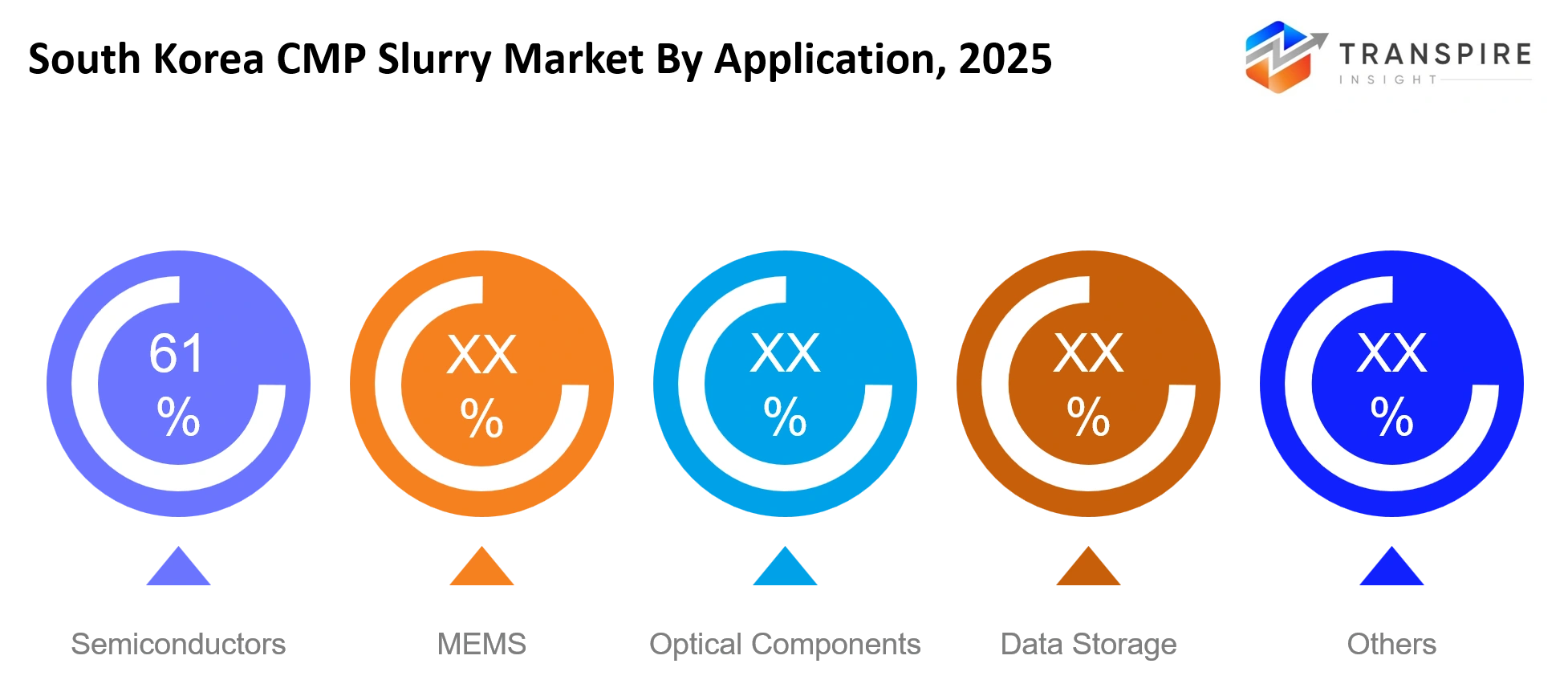
Semiconductors still play the main role, because CMP slurry is used to make wafer surfaces flatter during chip fabrication, you know, the usual kind of prep. MEMS applications also lean on slurry for micro device surface refinement, it’s kind of a subtle step but it matters. Optical components need polishing too, to boost clarity, and overall performance, so the light behaves. Data storage devices keep depending on CMP for steadier behavior and better density. Beyond that there are specialized industrial uses and electronic component manufacturing where the same idea shows up again.
Semiconductor use will keep leading as advanced chip production ramps up in South Korea, seems pretty straightforward. MEMS use is growing at a slower pace since sensor demand is expanding across automotive and electronics. Optical component usage stays fairly stable, helped by precision device manufacturing. Data storage will remain important due to continuing memory innovation cycles. In general, application demand is closely tied to fabrication upgrades and the rising complexity of wafers, which is where everything gets tricky.
By Material :
Copper CMP backs metal interconnect formation in semiconductor devices and keeps those conductive routes, rather smooth. Tungsten CMP gets used when contact plug formation is needed, for steadier electrical connections that hold up. STI CMP kind of helps separate device regions on silicon wafers, so isolation actually happens. Dielectric CMP supports insulating layer planarization too, so the surface stays even. Then there are other material processes that cover special semiconductor fabrication needs too, like the usual “not everything fits one step” situation.
Copper CMP stays really important as demand keeps climbing for advanced logic chips. Tungsten CMP keeps getting steady use in memory and logic devices, and it does that quietly, day after day. STI CMP also plays a key role in outlining transistor structures in today’s chips, without which the whole layout falls apart. Dielectric CMP demand ramps up as multi layer chip designs expand and the stacks get thicker. Each materials segment supports different fabrication steps, and when you combine them the total demand should keep increasing as chip complexity grows across South Korea.
By End User :
Foundries use CMP slurry a lot, for huge scale semiconductor manufacturing and also advanced node work. IDMs handle both the design and the making, and in practice they run slurry through their integrated production lines. OSAT companies, you know, apply CMP processes during packaging and testing phases. And then there are other end users too, like research labs, and some specialized electronic manufacturers that want a very fine surface finish.
In general, foundries dominate usage because the chip volumes are enormous, plus there’s heavy investment in new fabrication. IDMs still keep strong demand, since the integrated flow basically needs slurry to stay consistent over several different process steps. OSAT companies are growing their use too, especially as advanced packaging becomes more important for how the chip performs. Other end users are still smaller right now, but they should expand slowly as specialized technology develops, and as research driven semiconductor innovation picks up in South Korea.
What are the Key Use Cases Driving the South Korea CMP Slurry Market?
In the South Korea CMP Slurry Market, the dominant use case is mostly tied to advanced semiconductor wafer planarization, and slurry is kind of used to level out silicon and metal layers while the chip is being made, so the surface gets smoother. Demand is strongest in the high volume manufacturing lines, since the newer, smaller nodes call for extremely fine surface control, to keep both performance and yield stable.
After that, secondary use cases are growing too, mainly in advanced packaging and memory device refinement. This growth is especially visible in foundries and IDMs that make DRAM, NAND, and also these heterogeneous chip structures. Even OSAT companies are leaning on CMP processes more often, because chip stacking and integration keep increasing across consumer electronics and computing hardware, you know.
On the emerging side, people are looking at silicon photonics and high performance sensor fabrication. There the goal is ultra flat surfaces for better optical signal accuracy. Research driven semiconductor labs are also testing new slurry formulations for next generation AI chips, and that should, over time, widen adoption beyond the classic wafer manufacturing scope.
|
Report Metrics |
Details |
|
Market size value in 2025 |
USD 255.1 Million |
|
Market size value in 2026 |
USD 279.6 Million |
|
Revenue forecast in 2033 |
USD 531.1 Million |
|
Growth rate |
CAGR of 9.60% from 2026 to 2033 |
|
Base year |
2025 |
|
Historical data |
2021 - 2024 |
|
Forecast period |
2026 - 2033 |
|
Report coverage |
Revenue forecast, competitive landscape, growth factors, and trends |
|
Country scope |
South Korea |
|
Key company profiled |
Cabot Microelectronics, Fujimi, Resonac, BASF, Entegris, Merck KGaA, DuPont, Samsung SDI Materials, Soulbrain, KC Tech, SK Materials, Versum Materials, Hitachi Chemical, JSR, Saint-Gobain |
|
Customization scope |
Free report customization (country, regional & segment scope). Avail customized purchase options to meet your exact research needs. |
|
Report Segmentation |
By Type (Silica Slurry, Alumina Slurry, Ceria Slurry, Diamond Slurry, Others) | By Application (Semiconductors, MEMS, Optical Components, Data Storage, Others) | By Material (Copper CMP, Tungsten CMP, STI CMP, Dielectric CMP, Others) | By End User (Foundries, IDMs, OSAT Companies, Others) |
Which Regions are Driving the South Korea CMP Slurry Market Growth?
Seoul Capital Region is kind of leading the South Korea CMP Slurry Market because it has a dense crowd of semiconductor fabs, R&D neighborhoods, and advanced materials suppliers. Most production clusters sit around Gyeonggi Province, and that keeps the demand rolling for high purity slurry, used in sub-5nm wafer processing. On top of that there is strong government support for semiconductor self sufficiency, plus very close integration between chipmakers and material vendors , which basically keeps the region on top. The area also gets faster qualification cycles and a lot of tight collaboration between fabs and chemical sellers.
Then you have the southeastern part, more or less centered around Busan and Ulsan, which adds momentum in a steadier way. It leans on its industrial backbone and export tied manufacturing setup. In contrast to the Seoul region’s more innovation hungry demand, this area puts emphasis on production stability and supply chain continuity for more mature semiconductor processes. Raw chemical inputs get shipped reliably, and industrial logistics run efficiently, so slurry supply stays consistent. Also long term agreements with electronics and materials manufacturers help keep revenue predictable, even when conditions are not perfect.
The fastest growing push comes from the newer semiconductor industrial zones in central provinces, where new fab builds are happening and government backed investment programs show up. With recent infrastructure upgrades , and incentives that encourage locally sourced materials, slurry adoption in these zones has sped up. So, this looks like a decentralization of semiconductor output away from the old flagship clusters. During 2026–2033, that movement should open fresh entry points for suppliers trying to form early partnerships with upcoming fabrication facilities.
Who are the Key Players in the South Korea CMP Slurry Market and How Do They Compete?
Competition within the South Korea CMP Slurry Market is kinda moderately consolidated, not a total free for all, but also not fully locked down. A handful of global chemical and material companies control the most advanced formulations while smaller players usually end up in a more niche role, or they chase cost-focused segments. In the end, tech leadership kind of rules everything, because fabs need ultra-high purity and slurry customization that is really tied to the exact process, not just generic recipes. Incumbents also tend to stay ahead through long qualification cycles and co-development work with semiconductor makers, instead of playing pure price games only.
DuPont competes by leaning into high-performance material engineering, and also by going deep with the semiconductor process development teams. It differentiates via advanced slurry formulations built for sub-5nm nodes, and the edge comes from staying closely aligned with leading foundries, basically for early-stage process validation.
Entegris meanwhile leans heavily into contamination control plus ultra-pure material delivery systems, and that makes it strong in precision-driven fabrication environments. Its advantage is often tied to filtration and chemical handling technologies, since those can reduce defect risks inside CMP operations. They also keep expanding through partnerships with advanced chip manufacturers, rather than working in isolation.
Fujimi Incorporated specializes in abrasive slurry chemistry, and it keeps a solid footing in polishing efficiency, especially for memory chip production. Their direction centers on material innovation for more consistent surface finishing, and growth is supported by collaboration with Asian semiconductor fabs, not just domestic customers.
Cabot Microelectronics, now part of broader advanced materials portfolios, competes with a mix of scale and process optimization know-how. It supports its position by supplying high-volume CMP consumables, and it expands through long-term supply agreements with global semiconductor manufacturers.
Company List
- Cabot Microelectronics
- Fujimi
- Resonac
- BASF
- Entegris
- Merck KGaA
- DuPont
- Samsung SDI Materials
- Soulbrain
- KC Tech
- SK Materials
- Versum Materials
- Hitachi Chemical
- JSR
- Saint-Gobain
Recent Development News
In December 2025, Fujimi Corporation expanded its advanced abrasive slurry production capacity in Asia to support rising demand from memory chip manufacturers in South Korea and Taiwan. The expansion focused on improving supply stability for sub-5nm and 3D NAND process chemistries and reducing lead time constraints for semiconductor fabs.
Source https://www.reanin.com/reports/
In January 2026, DuPont announced expansion of its advanced semiconductor materials collaboration with major Asian foundry partners. The development focused on improving next-generation CMP slurry formulations for sub-5nm and 3D NAND production, strengthening process stability and wafer yield in high-volume manufacturing lines.
Sourcehttps://www.reanin.com/
What Strategic Insights Define the Future of the South Korea CMP Slurry Market?
South Korea CMP Slurry Market is kinda moving, toward a more specialized setup where the demand is basically funneled into ultra advanced semiconductor nodes and different heterogeneous integration platforms. The overall growth path gets shaped by fast scaling of AI chips, 3D NAND stacks, and sub-3nm logic output, and in turn it pushes fabs to lean on precision engineered slurry systems, instead of using more standard formulations. Over time this change should keep lifting product worth per wafer, while also making supplier qualification a lot stricter across the whole ecosystem.
There is also a quieter kind of risk that is easy to overlook, like raw material concentration especially for high purity abrasives and specialty chemicals that are pulled from a narrower supplier network. If something goes sideways upstream in chemical refining, or if export restrictions tighten, fabrication throughput can get slowed down, even if downstream chip demand is still strong. So you get this hidden supply side volatility that shows up later, not at the headline level.
At the same time there is an emerging chance too, in the form of localized co-development hubs inside new semiconductor clusters that are being built outside the usual production areas in South Korea. Those hubs let slurry teams co engineer materials with fabs directly during early process design, so qualification timelines can shrink, and things get tested sooner. Market participants should probably put money into on-site technical collaboration groups, to grab early design wins, and to secure longer term supply arrangements before the industry standards fully solidify.
South Korea CMP Slurry Market Report Segmentation
By Type
- Silica Slurry
- Alumina Slurry
- Ceria Slurry
- Diamond Slurry
By Application
- Semiconductors
- MEMS
- Optical Components
- Data Storage
By Material
- Copper CMP
- Tungsten CMP
- STI CMP
- Dielectric CMP
By End User
- Foundries
- IDMs
- OSAT Companies
Frequently Asked Questions
Find quick answers to common questions.
The South Korea CMP Slurry Market size is USD 531.1 Million in 2033.
Key segments for the South Korea CMP Slurry Market are By Type (Silica Slurry, Alumina Slurry, Ceria Slurry, Diamond Slurry, Others) | By Application (Semiconductors, MEMS, Optical Components, Data Storage, Others) | By Material (Copper CMP, Tungsten CMP, STI CMP, Dielectric CMP, Others) | By End User (Foundries, IDMs, OSAT Companies, Others).
Major South Korea CMP Slurry Market players are Cabot Microelectronics, Fujimi, Resonac, BASF, Entegris, Merck KGaA, DuPont, Samsung SDI Materials, Soulbrain, KC Tech, SK Materials, Versum Materials, Hitachi Chemical, JSR, Saint-Gobain.
The South Korea CMP Slurry Market size is USD 255.1 Million in 2025.
The South Korea CMP Slurry Market CAGR is 9.60% from 2026 to 2033.
- Cabot Microelectronics
- Fujimi
- Resonac
- BASF
- Entegris
- Merck KGaA
- DuPont
- Samsung SDI Materials
- Soulbrain
- KC Tech
- SK Materials
- Versum Materials
- Hitachi Chemical
- JSR
- Saint-Gobain
About the Authors

Pankaj Ghogare Patil
I am Pankaj Ghogare Patil, a Senior Research Analyst at Transpire Insight, specializing in the Pharmaceutical, Chemicals & Materials, Healthcare IT, and Biotechnology industry. My expertise lies in conducting comprehensive market research, analyzing industry trends, evaluating competitive landscapes, and translating complex data into actionable insights. At Transpire Insight, I closely follow emerging technologies, regulatory developments, and market innovations to create accurate, well-researched, and informative content that helps businesses and professionals make informed decisions. I am committed to producing credible, evidence-based articles that reflect industry best practices while making technical topics accessible and valuable for a broad audience.

Chakradhar Khansole
Chakradhar serves as the Research Director at Transpire Insight, bringing over 8 years of experience in technology, innovation, and strategic market intelligence. He specializes in transforming complex market data into actionable business insights that enable organizations to make informed, growth-oriented decisions. Recognized for his strategic vision and analytical expertise, Chakradhar leads high-impact research initiatives, delivering comprehensive market assessments, competitive intelligence, and forward-looking industry analysis.
Recently Published Reports
-
May 2026
Healthcare Polymer Packaging Market
Healthcare Polymer Packaging Market Size, Share & Analysis Report By Packaging Type (Syringes, IV Bottles and Pouches, Clamshells, Blisters, Bottles & Jars, Containers, Tubes, IV Parental Packaging, Others), By Type (Regulated, Non-regulated), By Polymer Type (LDPE (Low-Density Polyethylene), HDPE (High-Density Polyethylene), Homo-polymer (Homo), Random Copolymer (Random), Block Copolymer (Block), PET, Polystyrene, Polyvinyl Chloride, Polyamide/EVOH, Others), and Geography (North America, Europe, Asia-Pacific, Middle East and Africa, South and Central America), 2021 - 2031
-
Apr 2026
Hydrophilic Tape (Waterstop) Market
Hydrophilic Tape (Waterstop) Market Size, Share & Analysis Report By Type (Bentonite-Based Hydrophilic Tape, Rubber-Based Hydrophilic Tape), By Application (Residential Buildings, Commercial Buildings, Infrastructure Projects), and Geography (North America, Europe, Asia-Pacific, Middle East and Africa, South and Central America), 2021 - 2031
-
Apr 2026
Metalens Market
Metalens Market Size, Share & Analysis Report By Type (Visible Light Metalens, and Infrared Metalens), By Application (Consumer Electronics, Automotive Electronics, Industrial, Medical, and Others), and Geography (North America, Europe, Asia-Pacific, Middle East and Africa, South and Central America), 2021 - 2031
-
Apr 2026
PBT Resin Market
PBT Resin Market Size, Share & Analysis Report By Type (Reinforced PBT Resin, Unreinforced PBT Resin), By Processing Method (Injection Molding, Extrusion, Blow Molding, Others), By End-User (Automotive, Electrical & Electronics, Consumer Appliances, Industrial Machinery, Medical Devices, Packaging, Others), and Geography (North America, Europe, Asia-Pacific, Middle East and Africa, South and Central America), 2021 - 2031