
Global Thin Film Encapsulation Market Size & Forecast:
- Global Thin Film Encapsulation Market Size 2025: USD 170.2 Million
- Global Thin Film Encapsulation Market Size 2033: USD 694.8 Million
- Global Thin Film Encapsulation Market CAGR: 19.17%
- Global Thin Film Encapsulation Market Segments: By Type (Organic Encapsulation, Inorganic Encapsulation, Hybrid Encapsulation, Multilayer Encapsulation, Flexible Encapsulation, Others); By Application (OLED Displays, Flexible Electronics, Solar Cells, Wearable Devices, Medical Devices, Others); By End-User (Electronics Manufacturers, Semiconductor Companies, Display Manufacturers, Others); By Technology (ALD Technology, PECVD Technology, Inkjet Encapsulation, Others).
Global Thin Film Encapsulation Market Summary:
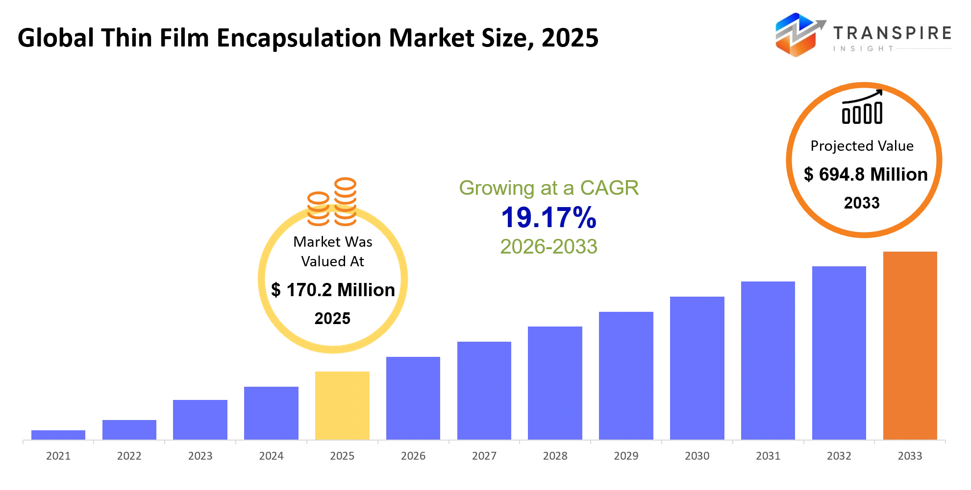
As per Transpire Insight Analysis, the global thin film encapsulation market size is estimated at USD 170.2 Million in 2025 and is anticipated to reach USD 694.8 Million by 2033, growing at a CAGR of 19.17% from 2026 to 2033.
This dynamic industry develops ultra-thin, nanoscale protective barriers designed to seal delicate organic optoelectronic components from degrading effects of air exposure. Over the past few years, the market has completely discarded heavy, rigid glass packaging to undergo a structural technological shift toward flexible, multi-layered organic and inorganic coatings.
A major real-world trigger behind this growth is the massive commercial production of foldable smartphones, rollable TVs, and curved wearable screens that fail immediately if moisture or oxygen penetrates their active layers. Consequently, display manufacturers are forced to replace standard sealing methods with advanced atomic layer deposition (ALD) and inkjet printing setups to deposit microscopic, flexible barrier stacks that preserve device lifespans without adding physical bulk.
Key Market Insights:
The global thin film encapsulation market - fundamentally shifting from rigid glass configurations to ultra-thin, nano-layered coating architectures that dynamically bend without fracturing. Driven by the mass adoption of foldable hardware, electronics manufacturers are replacing standard edge-sealing techniques with high-precision atomic layer deposition (ALD) and inkjet printing setups to deposit alternating organic-inorganic stacks that block degrading moisture.
- Locking down a dominant 58% global revenue share, OLED displays stand as the absolute operational foundation of the market, with manufacturing giants like LG Display continuously scaling up high-volume mass production of rollable and curved screens.
- Expanding at a distinct 15.6% CAGR, the flexible encapsulation segment is emerging as the primary technology type, driven by smartphone makers aggressively swapping standard rigid glass layers for elastic, multi-layer barrier stacks.
- Capturing an authoritative 42% share of worldwide revenue, the Asia Pacific region functions as the undisputed geographic manufacturing heavyweight, backed by massive cluster capital investments from semiconductor and display fabricators.
- Commanding a highly stable 29% market slice, North America continues to drive advanced material innovation, pushing aerospace and medical application teams to adopt localized encapsulation equipment for sensitive wearable sensor arrays.
- Representing 21% of total industry demand, the European theater relies heavily on strict product quality and green-building automotive regulations, propelling local premium car brands to adopt curved OLED instrument panels.
- Securing 15% of the market footprint, the flexible electronics segment is transitioning from simple printed circuit boards to highly complex, rollable logic matrices that require uniform, sub-nanometer barrier protection.
- Accounting for 10% of total procurement volume, the solar cells application segment is rapidly integrating thin-film encapsulation, utilizing barrier films from companies like Meyer Burger to seal fragile organic photovoltaics against outdoor weathering.
- Claiming an 8% market share, the wearable devices segment is moving toward continuous biometric monitoring, leveraging advanced equipment from Applied Materials to encapsulate microscopic health sensors without introducing structural rigidity.
- Accounting for 4% of total procurement volume, global medical device developers are aggressively adopting flexible encapsulation to protect bio-compatible, implantable electronic diagnostic tools from degrading physiological fluid exposure.
What are the Key Drivers, Restraints, and Opportunities in the Global Thin Film Encapsulation Market?
Driver
The market is expanding rapidly due to the commercial transition toward highly flexible, foldable, and rollable form factors in premium consumer electronics. Traditional rigid glass sealing covers are completely incompatible with screens that must fold or bend repeatedly without breaking. This shift was triggered by the massive commercial scaling of foldable smartphones and curved automotive IT dashboard displays, forcing display manufacturers to adopt nano-layered thin film architectures that protect delicate organic layers from atmospheric degradation. This operational urgency drives significant multi-layer deposition equipment sales as premium electronics brands aggressively phase out thick, rigid bezels to achieve true edge-to-edge, flexible panel designs.
In April 2026, semiconductor deposition leader Beneq launched its specialized custom ALD reactor configurations optimized for high-throughput, low-temperature spatial atomic layer deposition (SALD) processing on flexible substrates. This targeted product deployment directly helps global electronics manufacturers apply ultra-dense, pinhole-free inorganic moisture barriers onto heat-sensitive flexible OLED matrices, ensuring rapid barrier formation while maintaining pristine mechanical flexibility.
Restraint
The extreme capital installation cost of high-vacuum deposition cluster tools combined with low industrial fabrication yields persistently limits wide-scale commercial profitability. Achieving a critical water vapor transmission rate (WVTR) below 10^{-6} grams per square meter per day requires slow, tightly monitored atomic layer deposition cycles running inside highly complex, dust-free vacuum cleanrooms. This structural bottleneck persists because even microscopic particle contamination during the alternating organic-inorganic layering sequence creates tiny pinhole pathways, resulting in immediate dark-spot failures that wreck production yields for mid-tier display suppliers.
Opportunity
The most lucrative growth window lies in embedding high-barrier thin film encapsulation directly into the commercial manufacturing workflows of flexible, lightweight perovskite solar cells. Fusing transparent, nanolaminated hybrid encapsulation barriers with flexible plastic photovoltaic sheets allows energy developers to protect fragile organic solar materials from outdoor weathering without adding rigid glass overhead. This technological shift opens massive procurement streams across North America and Europe from construction firms seeking to deploy lightweight, flexible building-integrated photovoltaics (BIPV) across massive commercial roof spaces.
What Has the Impact of Artificial Intelligence Been on the Global Thin Film Encapsulation Market?
Artificial intelligence is actively transforming thin film encapsulation from an empirical, trial-and-error recipe process into an optimized, data-driven synthesis environment. Instead of executing hundreds of physical test runs to balance barrier thickness with structural flexibility, thin film developers embed deep learning algorithms directly into deposition control loops.
Operationally, AI deeply optimizes process parameters within high-vacuum atomic layer deposition (ALD) and plasma-enhanced chemical vapor deposition (PECVD) reactors. Neural networks analyze real-time plasma optical emission spectrums and pressure variables, dynamically fine-tuning precursor pulsing intervals to maintain angstrom-level thickness uniformity and flawless step coverage. Furthermore - AI brings massive predictive capabilities to quality assurance by processing multi-variate sensor logs to forecast water vapor transmission rate (WVTR) performance and pinpoint microscopic pinhole defects before physical aging tests conclude, drastically accelerating production throughput.
Key Market Trends:
The thin film encapsulation landscape is undergoing a profound structural evolution, shifting away from massive multi-layer material configurations toward hyper-dense, sub-micron single-chamber processing. Driven by extreme engineering pressures to thin down foldable screens, display fabricators are replacing slow, separate vacuum-to-atmosphere handling sequences with fully integrated, continuous-vacuum cluster tool steps that preserve delicate organic interfaces from microscopic particle defects.
- For years, panel manufacturers depended exclusively on a rigid, three-layer inorganic-organic-inorganic triad stack, but fabrication lines are rapidly transitioning toward zero-stress, ultra-thin two-layer nanolaminates to dramatically maximize panel foldability.
- Instead of running unmonitored material deposition cycles that risk localized layer mismatch, cleanroom operators are actively equipping atomic layer deposition (ALD) chambers with automated optical emission feedback loops to track angstrom-scale uniformity in real-time.
- Traditional manufacturing facilities historically separated plasma-enhanced chemical vapor deposition (PECVD) lines from organic inkjet printing modules, but modern fabs are aggressively swapping them for inline, fully closed vacuum cluster systems to guarantee contamination-free panel transfers.
- To avoid severe internal film stress and subsequent layer cracking during aggressive mechanical bending, process engineers are moving away from traditional pure alumina barriers to adopt alternating Al2O3/ZrO2 hybrid atomic-layer configurations.
- Rather than deploying thick, localized edge-sealing adhesives around active electronic boundaries, display developers are transitioning toward uniform, edge-to-edge thin-film spatial ALD coatings to permanently lock out moisture molecules without increasing bezel thickness.
- Commercial consumer tech brands are thinking way beyond standard flat smartphones, pushing a sweeping industry shift toward multi-fold screens, rollable tablet form factors, and curved automotive cockpits that require highly elastic, low-Young's-modulus barrier packaging.
- Instead of relying entirely on standard high-temperature chemical reactions that degrade fragile organic light-emitting polymers, equipment suppliers are deeply embedding low-temperature, radical-assisted deposition protocols that run strictly below 100 degrees Celsius.
- To satisfy intense automotive tier-one environmental reliability standards, thin-film material producers are ditching basic single-layer silicon nitride coatings in favor of filtered cathodic vacuum arc (FCVA) oxides to ensure superior thermal endurance under accelerated aging.
- Local microelectronic packaging hubs are completely overhauling their fabrication routing methods, pushing a major move toward continuous roll-to-roll (R2R) spatial ALD lines to eliminate production throughput bottlenecks across flexible printed circuit lines.
Global Thin Film Encapsulation Market Segmentation
By Type
Flexible encapsulation and multilayer encapsulation pull in the lion's share of cash in this market simply because manufacturing and scaling them requires specialized high-vacuum cluster tool infrastructure. At the same time, hybrid encapsulation is growing incredibly fast, accelerating at an explosive, market-leading CAGR. The real reason behind this setup comes down to extreme mechanical stress in foldable devices and the urgent need to preserve delicate organic layers from atmospheric degradation over long product lifespans. High-density multilayer and flexible encapsulation are absolutely essential to prevent rapid moisture penetration and eliminate internal film stress that causes layer cracking during aggressive bending. On the flip side, hybrid varieties are booming because of a massive engineering behavioral push, forcing display and consumer electronic brands to source single-chamber solutions that combine the flexibility of polymers with the dense barrier properties of ceramics. Looking ahead, material handling will merge completely with precision inline chemical deposition. Encapsulation equipment suppliers will have no choice but to build out automated, closed-loop cluster tools and low-stress hybrid molecular structures to hit tough device durability and ultra-thin bezel design standards.
By Application
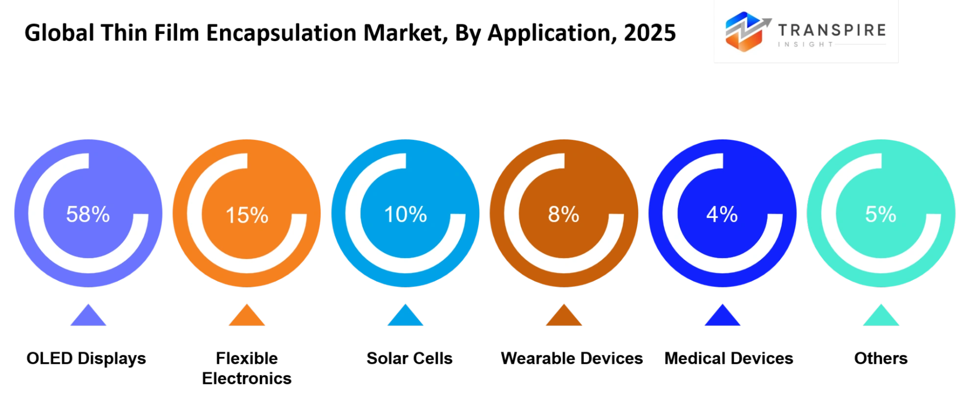
OLED displays remain the absolute heavyweights of this industry, locking down a dominant 58% share of all global revenue. Flexible electronics applications follow behind at 15%, with solar cells sitting at 10%, wearable devices at 8%, medical devices at 4%, and other industrial niches claiming 5%. This massive concentration isn't going anywhere because master panel fabrication facilities and global consumer tech brands buy deposition equipment and materials in massive institutional volumes to keep up with everyday commercial smartphone and TV production schedules. However, things get really interesting in the energy and medical space, where solar cells and implantable diagnostics stand out as highly lucrative pockets as next-generation perovskite solar labs and bio-compatible device designers demand stable, lightweight active compounds. Moving forward, everything suppliers produce will need to focus on sub-nanometer thickness uniformity and low-temperature processing. Encapsulation providers will have to balance two main workloads: supplying massive, cost-efficient multilayer deposition systems to traditional commercial display fabs while refining high-purity, ultra-flexible atomic layer deposition tools for the rapidly expanding flexible photovoltaic, medical sensor, and wearable electronics industries.
By End-User
Display manufacturers remain the absolute anchor of day-to-day market demand due to their massive, predictable bulk procurement power for high-volume consumer panels. Meanwhile, semiconductor companies and specialized electronics manufacturers are stepping in as high-value, fast-growing secondary end-users. The growth pattern here depends entirely on how quickly electronic form factors evolve and how strictly manufacturers need to track raw material purity and barrier water vapor transmission rates. Large display manufacturers rely on massive, standardized multi-year capital equipment contracts to secure stable fab capacity, while semiconductor and electronics makers look for unique, low-temperature coating profiles and specialized substrate certifications. Moving forward, major equipment and material suppliers won't be able to survive just by selling standalone deposition tools. Long-term success will mean locking down fully integrated technology and licensing agreements. Equipment providers will need to bundle the actual physical cluster setups with ongoing formulation and software support, offering customized precursor gas chemistries, automated inline thickness consistency tracking, and precise yield-optimization analytics to meet changing consumer tech demands.
By Technology
PECVD technology and inkjet encapsulation hold a major portion of the operational footprint because of their historical reliability in rapidly depositing thick organic decoupling layers. Concurrently, ALD technology represents the undisputed market accelerator, charging ahead as the fastest-growing technology segment. The growth logic here is entirely driven by the transition from micro-scale protective layers to hyper-dense, angstrom-level barrier perfection. Legacy encapsulation setups fail because line-of-sight deposition cannot provide flawless step coverage over complex, vertical step heights, leading to catastrophic moisture leaks and dead pixels. ALD technology resolves this structural vulnerability by operating as a self-limiting chemical reaction that builds unblinking, pinhole-free inorganic barriers atomic layer by atomic layer. Looking ahead, software and hardware providers will be forced to move past separate, multi-chamber processing sequences. Future market dominance will belong to platforms that utilize predictive spatial ALD networks capable of delivering high-throughput, continuous-vacuum roll-to-roll operations, enabling creators to instantly apply ultra-dense barrier coatings onto heat-sensitive flexible substrates without breaking vacuum lines.
What are the Key Use Cases Driving the Global Thin Film Encapsulation Market?
The dominant deployment of thin film encapsulation infrastructure centers heavily on the preservation of high-end consumer electronics within the premium OLED displays segment. In these high-volume fabrication lines, manufacturers utilize precise atomic layer deposition (ALD) and inkjet printing systems to coat delicate organic light-emitting polymers with microscopic, multi-layered moisture barriers. This critical coating step prevents rapid atmospheric degradation, effectively eliminating dead-pixel development while enabling smartphones and rollable televisions to fold repeatedly without experiencing layer fracture.
Beyond traditional display environments, applications are rapidly expanding across high-performance flexible electronics and smart wearable devices. Hardware engineers utilize low-temperature plasma-enhanced chemical vapor deposition (PECVD) to seal elastic logic circuits and flexible printed circuit boards, safeguarding sensitive consumer electronics against sweat and moisture infiltration without adding rigid geometric bulk.
Emerging use cases are gaining significant traction within the medical devices sector and advanced renewable energy frameworks - specifically targeting implantable biosensors and next-generation perovskite solar cells. Instead of relying on thick glass packaging, biomedical and solar developers deploy pinhole-free hybrid encapsulation barriers to protect fragile, bio-compatible sensor matrices from harsh physiological fluids and outdoor weathering, shifting the industry toward highly durable, low-profile device integration.
|
Report Metrics |
Details |
|
Market size value in 2025 |
USD 170.2 Million |
|
Market size value in 2026 |
USD 203.5 Million |
|
Revenue forecast in 2033 |
USD 694.8 Million |
|
Growth rate |
CAGR of 19.17% from 2026 to 2033 |
|
Base year |
2025 |
|
Historical data |
2021 - 2024 |
|
Forecast period |
2026 - 2033 |
|
Report coverage |
Revenue forecast, competitive landscape, growth factors, and trends |
|
Regional scope |
United States; Canada; Mexico; United Kingdom; Germany; France; Italy; Spain; Denmark; Sweden; Norway; China; Japan; India; Australia; South Korea; Thailand; Brazil; Argentina; South Africa; Saudi Arabia; United Arab Emirates |
|
Key company profiled |
Samsung SDI, LG Display, Applied Materials, Universal Display Corporation, Veeco Instruments, Kateeva, Beneq, Meyer Burger, Aixtron, ULVAC, Canon Tokki, Toray Industries, ASM International, Encapsulix, Optomec. |
|
Customization scope |
Free report customization (country, regional & segment scope). Avail customized purchase options to meet your exact research needs. |
|
Report Segmentation |
By Type (Organic Encapsulation, Inorganic Encapsulation, Hybrid Encapsulation, Multilayer Encapsulation, Flexible Encapsulation, Others); By Application (OLED Displays, Flexible Electronics, Solar Cells, Wearable Devices, Medical Devices, Others); By End-User (Electronics Manufacturers, Semiconductor Companies, Display Manufacturers, Others); By Technology (ALD Technology, PECVD Technology, Inkjet Encapsulation, Others). |
Which Regions Are Driving the Global Thin Film Encapsulation Market Growth?
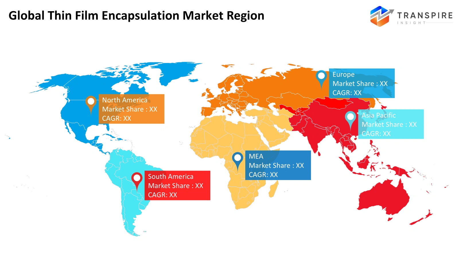
The Asia-Pacific region maintains a commanding grip on the global thin film encapsulation market, capturing a dominant 42% of all worldwide industry revenue. This geographic hegemony is heavily driven by a massive concentration of premier panel fabricators, semiconductor foundries, and consumer electronics consumer clusters across South Korea, China, and Japan. The regional ecosystem is structurally supported by aggressive state-backed industrial manufacturing subsidies and extensive multi-billion-dollar corporate investments into high-volume manufacturing hubs. Consequently, integrating specialized thin film barriers has become an absolute operational mandate for East Asian display giants seeking to scale the mass production of next-generation flexible smartphones and curved electronic devices.
Europe serves as a highly stable, predictable secondary pillar for the global market, locking down an essential 21% share of total industry demand. While the Asia-Pacific market concentrates heavily on high-volume consumer smartphone panels, European system adoption is driven entirely by its luxury automotive electronics, flexible batteries, and industrial lighting sectors. This regional market stability is structurally insulated by rigid vehicular safety standards and regional manufacturing quality frameworks that force automotive component makers to deploy highly reliable electronic shielding. To maintain strict corporate compliance and ensure long-term product endurance, European tier-one automotive engineering firms steadily contract for robust multi-layer barrier films equipped with specialized thermal dissipation properties.
North America has emerged as the fastest-growing territory globally, accelerating at a market-leading 14.8% CAGR while securing a critical 29% of the overall market revenue footprint. This sudden structural shift is driven by rapid technological breakthroughs in specialized microelectronics and an explosive medical wearable device boom across the United States and Canada. Historically, the region focused on importing finished panels, but it has now rapidly pivoted into a primary developer of indigenous, high-purity nanolaminated hybrid encapsulation materials to insulate fragile military and biomedical sensors. Looking ahead, future procurement in this booming corridor relies entirely on deploying advanced, sub-nanometer equipment platforms capable of generating zero-stress protective barriers over highly intricate, three-dimensional chip configurations.
In June 2026, North American semiconductor equipment leader Applied Materials Inc. expanded its flagship AKT Enflexor thin-film encapsulation product line by integrating unique high-precision vision alignment technologies. This specialized hardware deployment explicitly targets the rapidly expanding North American aerospace and flexible sensor production sectors, allowing device fabricators to execute maskless, low-temperature barrier deposition cycles that radically reduce photolithography processing costs while guaranteeing maximum moisture protection.
Who are the Key Players in the Global Thin Film Encapsulation Market and How Do They Compete?
The global thin film encapsulation market features intense technical rivalry between advanced semiconductor equipment corporations and specialized electronic material patent-holders. Competition is structurally anchored around maximizing water vapor transmission barrier density while maintaining rapid substrate processing speeds, forcing manufacturers to move past basic standalone equipment sales to deliver highly complex, inline production line solutions. Applied Materials Inc. leverages a high-volume industrial innovation strategy via its specialized AKT vacuum cluster frameworks, dominating high-throughput lines by integrating flexible packaging steps directly with high-efficiency plasma-enhanced chemical vapor deposition (PECVD) layers across premier East Asian display fabrication complexes. Operating on an intellectual property licensing model, Universal Display Corporation (UDC) differentiates its market position through its signature UNIVERSALBARRIER® platforms, which combine hybrid organic-inorganic properties to achieve multi-layer protection down to a sub-1mm bend radius without physical cracking. Meanwhile, Veeco Instruments Inc. maintains a highly targeted, niche engineering focus centered on supreme high-vacuum perfection, separating itself through specialized batch atomic layer deposition (ALD) platforms engineered to deploy low-temperature, damage-free protective coatings over sensitive biomedical sensors and next-generation micro-LED architectures.
Company List
- Samsung SDI
- LG Display
- Applied Materials
- Universal Display Corporation
- Veeco Instruments
- Kateeva
- Beneq
- Meyer Burger
- Aixtron
- ULVAC
- Canon Tokki
- Toray Industries
- ASM International
- Encapsulix
- Optomec
Recent Development News
In September 2025, American display inkjet manufacturing leader Kateeva Inc. officially expanded its long-term technology partnership with high-purity nano-material innovator Pixelligent Technologies. This strategic development focuses on co-optimizing an inkjet-printed organic planarization layer over advanced microlens arrays, allowing display fabs to perfectly combine light-output efficiency enhancements with ultra-thin, crack-resistant thin film encapsulation steps on mobile phone production lines.
Source: https://kateeva.com
In March 2026, South Korean equipment innovator STI Co., Ltd. officially secured a major commercial contract to supply automated cleanroom ink supply systems directly to a premier display manufacturer's next-generation OLED production facility. This technical deployment guarantees continuous, bubble-free fluid transport for precision inkjet printing modules, enabling the high-throughput application of organic decoupling layers required to seal ultra-flexible display panels without introducing particle contamination.
Source: http://www.thelec.net
In July 2026, the global Thin Films Society commenced its 11th international conference assembly in Singapore, dedicating a major specialized industrial symposium to structural engineering breakthroughs in atomic layer deposition (ALD). The academic-industry collaborative showcase unveiled multi-layered organic-inorganic molecular sieves that effectively minimize internal film stress, giving microelectronic package designers an optimized blueprint to construct flexible, pinhole-free hybrid barriers down to sub-micron geometric bounds.
Source: https://conference.thinfilms.sg
What Strategic Insights Define the Future of the Global Thin Film Encapsulation Market?
The thin film encapsulation landscape is rapidly moving toward integrated, single-chamber hybrid nanolaminates to eliminate processing bottlenecks associated with traditional multi-layer stacks. A critical hidden risk in this progression is the interface degradation vulnerability, where microscopic chemical mismatches between alternating organic and inorganic materials cause micro-delamination when subjected to aggressive, repeated folding cycles.
Conversely, an exceptional emerging opportunity lies in the deployment of spatial ALD (sALD) platforms within the roll-to-roll production of perovskite solar cells and flexible medical sensors. To capitalize on this shift, manufacturing leaders must discard isolated equipment procurement models. Instead, they should execute structured co-development frameworks that bundle inline, machine-learning-driven defect inspection algorithms with low-temperature chemical precursor packages, locking down the sub-nanometer consistency required for high-yield, flexible microelectronics manufacturing.
Key Segmentations are:
By Type
- Organic Encapsulation
- Inorganic Encapsulation
- Hybrid Encapsulation
- Multilayer Encapsulation
- Flexible Encapsulation
- Others
By Application
- OLED Displays
- Flexible Electronics
- Solar Cells
- Wearable Devices
- Medical Devices
- Others
By End-User
- Electronics Manufacturers
- Semiconductor Companies
- Display Manufacturers
- Others
By Technology
- ALD Technology
- PECVD Technology
- Inkjet Encapsulation
- Others
Regional Outlook
North America
- United States
- Canada
- Mexico
Europe
- Germany
- United Kingdom
- France
- Spain
- Italy
- Rest of Europe
Asia Pacific
- Japan
- China
- Australia & New Zealand
- South Korea
- India
- Rest of Asia Pacific
South America
- Brazil
- Argentina
- Rest of South America
Middle East & Africa
- Saudi Arabia
- United Arab Emirates
- South Africa
- Rest of the Middle East & Africa
Frequently Asked Questions
Find quick answers to common questions.
The global thin film encapsulation market size was valued at USD 170.2 Million in 2025 and is poised to reach USD 694.8 Million by 2033, expanding at a 19.17% CAGR.
Key segments for the global thin film encapsulation are Type (Organic Encapsulation, Inorganic Encapsulation, Hybrid Encapsulation, Multilayer Encapsulation, Flexible Encapsulation, Others), Application (OLED Displays, Flexible Electronics, Solar Cells, Wearable Devices, Medical Devices, Others), End-User (Electronics Manufacturers, Semiconductor Companies, Display Manufacturers, Others), and Technology (ALD Technology, PECVD Technology, Inkjet Encapsulation, Others).
Growth is primarily driven by the surging consumer demand for flexible OLED displays and foldable smartphones, rapid automotive adoption of curved cockpit screens, and advancements in low-temperature atomic layer deposition (ALD) techniques that protect heat-sensitive substrate components.
The global market is led by major manufacturers including Samsung SDI, LG Display, Applied Materials, Universal Display Corporation, Veeco Instruments, Kateeva, Beneq, Meyer Burger, Aixtron, ULVAC, Canon Tokki, Toray Industries, ASM International, Encapsulix, and Optomec.
Asia-Pacific holds a dominant 42% share of the global thin film encapsulation market, anchoring industry dynamics through its dense concentration of premier panel fabrication complexes in South Korea and China, aggressive state-backed electronics manufacturing subsidies, and massive corporate infrastructure expansions.
High-value commercial opportunities exist in rolling out automated spatial ALD (sALD) equipment lines optimized for continuous roll-to-roll (R2R) processing, alongside deploying zero-stress hybrid nanolaminated barriers for next-generation perovskite solar panels and implantable healthcare biosensors.
- Samsung SDI
- LG Display
- Applied Materials
- Universal Display Corporation
- Veeco Instruments
- Kateeva
- Beneq
- Meyer Burger
- Aixtron
- ULVAC
- Canon Tokki
- Toray Industries
- ASM International
- Encapsulix
- Optomec
About the Authors

Avinash Kumar
I’m Avinash Kumar, a Senior Research Analyst at Transpire Insight, with expertise in the Electronics and Semiconductor and Energy & Power industry. My work focuses on analyzing emerging technologies, market trends, industry developments, and innovation across these sectors. I specialize in transforming complex technical and market insights into clear, research-backed content that helps professionals, businesses, and decision-makers stay informed. Through continuous industry research and data-driven analysis, I strive to deliver accurate, reliable, and practical perspectives on the latest advancements shaping the semiconductor and energy landscape.

Chakradhar Khansole
Chakradhar serves as the Research Director at Transpire Insight, bringing over 8 years of experience in technology, innovation, and strategic market intelligence. He specializes in transforming complex market data into actionable business insights that enable organizations to make informed, growth-oriented decisions. Recognized for his strategic vision and analytical expertise, Chakradhar leads high-impact research initiatives, delivering comprehensive market assessments, competitive intelligence, and forward-looking industry analysis.
Recently Published Reports
-
Apr 2026
Fiber Optic Faceplates Market
Fiber Optic Faceplates Market Size, Share & Analysis Report By Type (< 300 mm2, 300-350 mm2, and > 350 mm2, By Application (Night Vision, Holographic Imaging, Medical, and Others), and Geography (North America, Europe, Asia-Pacific, Middle East and Africa, South and Central America), 2021 - 2031
-
Apr 2026
High Temperature Superconductors Market
High Temperature Superconductors Market Size, Share & Analysis Report By Type (1G HTS, and 2G HTS), By Application (Power Cable, Fault Current Limiter, and Transformer), and Geography (North America, Europe, Asia-Pacific, Middle East and Africa, South and Central America), 2021 - 2031
-
Apr 2026
Industrial Plugs and Socket Market
Industrial Plugs and Socket Market Size, Share & Analysis Report By Type (Industrial Plugs, Industrial Sockets), By Current (Up to 32 A, 32 to 125 A, Above 125 A), By Protection (Dustproof and Splash Proof, Waterproof, Explosion Proof), By End User (Heavy Industries, Oil and Gas, Chemicals and Pharmaceuticals, Power Generation, Others), and Geography (North America, Europe, Asia-Pacific, Middle East and Africa, South and Central America), 2021 - 2031
-
Apr 2026
InGaAs Avalanche Photodiodes Market
InGaAs Avalanche Photodiodes Market Size, Share & Analysis Report By Type (1100 - 1700 nm, and 1000 - 1600 nm), By Application (Missile Warning System, Muzzle Flash Detection, Wafer Defect Inspection, Laser Rangefinders, and Others), and Geography (North America, Europe, Asia-Pacific, Middle East and Africa, South and Central America), 2021 - 2031