

United Kingdom AI EDA Market Size & Forecast:
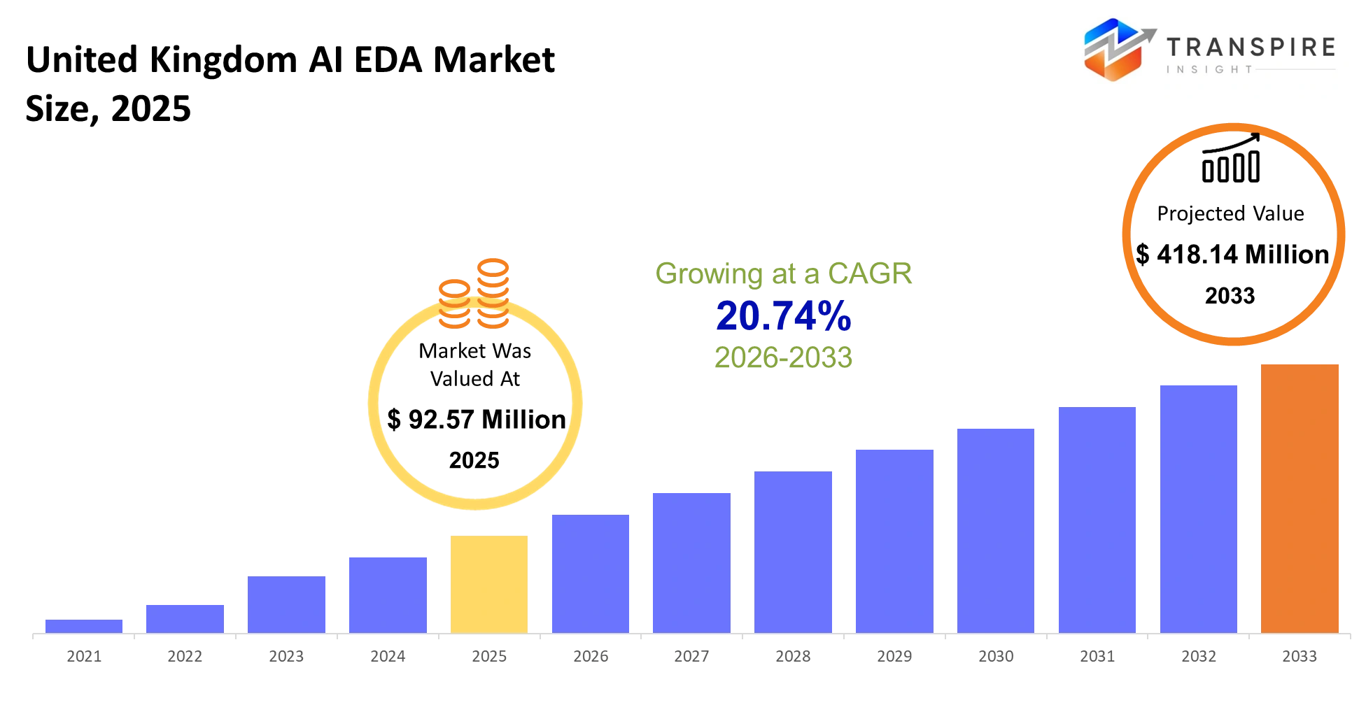
- United Kingdom AI EDA Market Size 2025: USD 92.57 Million
- United Kingdom AI EDA Market Size 2033: USD 418.14 Million
- United Kingdom AI EDA Market CAGR: 20.74%
- United Kingdom AI EDA Market Segments: By Component (Software Tools, AI Algorithms, Cloud Platforms, Verification Tools, Others); By Application (Chip Design, IC Verification, PCB Design, Semiconductor Manufacturing, Others); By Deployment (Cloud-based, On-premise, Hybrid Systems, Others); By End User (Semiconductor Companies, Electronics Manufacturers, Research Institutes, Others)
To learn more about this report,  Download Free Sample Report
United Kingdom AI EDA Market Summary
The United Kingdom AI EDA Market was valued at USD 92.57 Million in 2025. It is forecast to reach USD 418.14 Million by 2033. That is a CAGR of 20.74% over the period.
The United Kingdom AI EDA market is kinda reshaping the way semiconductor companies design, verify, and also optimize increasingly intricate chips, that show up in automotive electronics, telecom infrastructure, defense systems , and industrial automation. In real life, AI-enabled electronic design automation software cuts down on engineering bottlenecks by automating circuit validation, flagging possible design flaws earlier, and generally shrinking product development timelines for advanced nodes and more mixed, heterogeneous architectures.
Over the last five years, things have moved, sort of, from rules-based automation to machine learning driven design routines that can deal with huge data volumes coming from modern chip architectures. This shift got a faster push after the global semiconductor supply chain disruption made the risks of long design lead times pretty obvious, especially with that overseas fabrication dependence. Meanwhile the UK government’s semiconductor strategy, plus added investment in sovereign chip capabilities, has been encouraging more local R&D activity. And as AI workloads keep growing across data centers and edge computing, chipmakers are adopting AI EDA platforms to reduce tape-out failures, improve power efficiency, and reach the market quicker. That in turn supports licensing revenue and also helps lock in long-term software adoption.
Key Market Insights
- England kind of dominated the United Kingdom AI EDA Market, sitting at more than 68% market share in 2025, and that was largely held up by semiconductor R&D clusters around Cambridge , as well as London.
- Scotland then came in as the fastest-growing regional market in the 2025–2030 forecast window, mainly because photonics and advanced semiconductor research got heavier investments.
- In the South East England area there was a pretty sizable industry share contribution, tied to strong AI chip design demand from telecom groups and defense technology companies, too.
- On the software side, AI powered verification and validation tools did the most heavy lifting, taking nearly 34% of the revenue slice in 2025.
- Design automation software stayed as the second-largest segment, driven by more and more uptake of advanced node semiconductor architectures.
- Meanwhile, machine learning driven simulation tools started gaining ground, because they reduce chip tape-out errors and they can shorten engineering workflows by about 30%.
- Looking at application coverage, semiconductor manufacturing applications took roughly 41% of the United Kingdom AI EDA Market share in 2025.
- Automotive electronics is the one that showed up as the fastest-growing application track, sparked by EV adoption, ADAS integration , and the need for chips for autonomous driving systems.
- By end user, integrated device manufacturers led the pack with close to 46% revenue share, mostly due to high-volume chip development requirements.
- Fabless semiconductor companies were the fastest-growing end-user group across the forecast period, linked to quicker AI processor innovation cycles.
What are the Key Drivers, Restraints, and Opportunities in the United Kingdom AI EDA Market?
The most powerful driver pushing the United Kingdom AI EDA market forward is this pretty fast move toward AI focused semiconductor designs for data centers, automotive electronics, and edge computing. It really got louder after those global chip shortages, showed the money downside of slow design cycles and basically too little domestic semiconductor capacity. In response, UK chip teams and research groups started putting money into AI enabled electronic design automation tools, tools that cut down on verification duration, help with power tuning, and catch design flaws earlier while things are still flexible. And since semiconductor complexity keeps rising at advanced process nodes, companies end up leaning on AI EDA platforms, to shrink tape-out timelines and avoid expensive rework, which then supports more licensing income and longer term software subscription growth for EDA providers.
The markets biggest “stopper” is a shortage of deeply specialized semiconductor design engineers who can actually work at the same time with AI modeling and modern EDA processes. This issue isn’t something you can smooth over quickly, because training these people means years of academic education plus hands on design practice. Smaller UK semiconductor businesses often have a hard time fitting advanced AI EDA platforms into what they already do, so adoption stalls, and productivity improvements get capped. So overall you see slower commercialization for advanced chip programs, and that also keeps software spend lower at many mid sized design companies.
One of the clearer growth lanes is coming from the UKs expanding sovereign semiconductor roadmap, plus that university led chip innovation network. Research clusters around Cambridge and Scotland are drawing investment into photonics, compound semiconductor work, and AI accelerator development, and that combo could create more demand for specialized design automation.This creates pretty favorable condit ions for cloud based AI EDA platforms, that can actually support collaborative chip design across different and distributed engineering teams. You know, the sort of setup where people are not all in one place. Vendors that tuck in generative AI, predictive simulation, and automated verification, into scalable SaaS environments are in a good stance to grab long term growth, as domestic semiconductor R&D spending keeps expanding.
What Has the Impact of Artificial Intelligence Been on the United Kingdom AI EDA Market?
Artificial intelligence together with newer digital technologies are quietly shifting the way semiconductor companies in the United Kingdom design, validate, and push forward integrated circuits that are getting more and more complicated. In practice, AI-enabled electronic design automation platforms can handle several key jobs, like circuit verification, layout tweaking, timing assessment, and design rule checking, so a lot of the manual engineering work is reduced, sometimes quite a lot. Semiconductor teams then lean on machine learning approaches to watch over design integrity in real time, pick up weird anomalies earlier and even automate compliance follow-up for advanced process nodes as well as power efficiency requirements
Predictive analytics is also getting a special role, especially in high-performance chip work. AI models sift through old design records to estimate things like thermal patterns, signal integrity headaches, and even possible tape-out issues before fabrication starts. That method gives engineering teams a better shot at first-pass silicon success, and it can cut down on painful redesign cycles that cost both time and money. For cutting-edge chip programs, AI-assisted optimization can shorten verification schedules by as much as 30% and make better use of engineers in different locations, in other words across distributed teams. And cloud based collaborative design systems add more momentum, because they support real time simulation and let people manage their tasks remotely without constant back-and-forth.
Still, there is a catch: the high integration costs stay a major limitation. A number of mid sized semiconductor firms find it difficult to plug AI-driven EDA platforms into older, legacy design infrastructure, and the lack of access to huge proprietary training datasets can lower model accuracy, especially in highly specialized chip architectures.
Key Market Trends
- Since 2021, a bunch of UK semiconductor firms have kept leaning into AI - assisted verification tools. The main idea was to squeeze redesign costs a bit more, and also speed up the launch of advanced node products, not just in theory, but in practice too.
- After 2022, cloud-based EDA setups really took off. this was partly because engineering teams became more distributed, so they needed real time, kind of shared semiconductor design spaces.
- Also, in AI accelerator and data center chip work, buyer attention started moving. more folks wanted predictive simulation tools. those can catch thermal and power headaches earlier, before they turn into expensive surprises later.
- And then , after the global semiconductor shortages, UK policymakers basically upped domestic semiconductor spending. That ended up boosting demand for design ecosystems that are locally supported and AI-driven.
- On the automotive side, companies sped up using generative AI layout optimization tools. EV and ADAS chip complexity went up a lot after 2023, so the tooling demand followed pretty quickly.
- Synopsys and Cadence Design Systems also kept expanding their AI-enabled verification offerings. The point was to ride the growing need for faster tape-out cycles, so teams could ship sooner with less hassle.
- Semiconductor startups, increasingly moved away from purely on-premises infrastructure. they went toward SaaS based EDA platforms, mainly to reduce initial engineering loads and hardware costs, which is hard to ignore.
- Since 2020, machine-learning-led design automation has been shaving verification timelines. In complex AI processor programs, it reportedly dropped those timelines by about 30%, give or take.
- Meanwhile, UK research clusters around Cambridge and Scotland drew more investment in photonics and compound semiconductor areas. That seems to have strengthened regional take-up of AI EDA software, step by step.
- Lastly, many semiconductor manufacturers began weaving reinforcement learning techniques into their design workflows. The goal was better power optimization, and fewer engineering resource jams, sometimes referred to as bottlenecks in plain terms.
United Kingdom AI EDA Market Segmentation
By Component
Software tools grabbed the largest share of revenue in 2025, mainly because semiconductor companies leaned heavily on AI-enabled automation for layout work, timing assessment, and power tuning. Newer chip blueprints made verification way more complicated too, so engineering groups started preferring bundled EDA suites that can cut down design cycles and also reduce those expensive tape-out mishaps. Verification tools landed next as the second-largest segment, since makers face increasing pressure to boost first-time silicon outcomes for AI accelerators and automotive semiconductors.
After 2022, AI algorithms and cloud platforms picked up momentum more than before, as chip developers shifted toward predictive analytics and more cooperative remote design setups. Tools using machine-learning-based optimisation improved simulation precision, and helped spot defects faster across advanced nodes under 7 nm. During the forecast period, cloud-native EDA ecosystems are expected to pull in even more funding , because scalable compute lets teams run simulation jobs quicker and coordinate distributed engineering tasks. Meanwhile product teams and investors seem to like modular AI software frameworks, where generative AI can be folded into existing semiconductor processes.
By Application
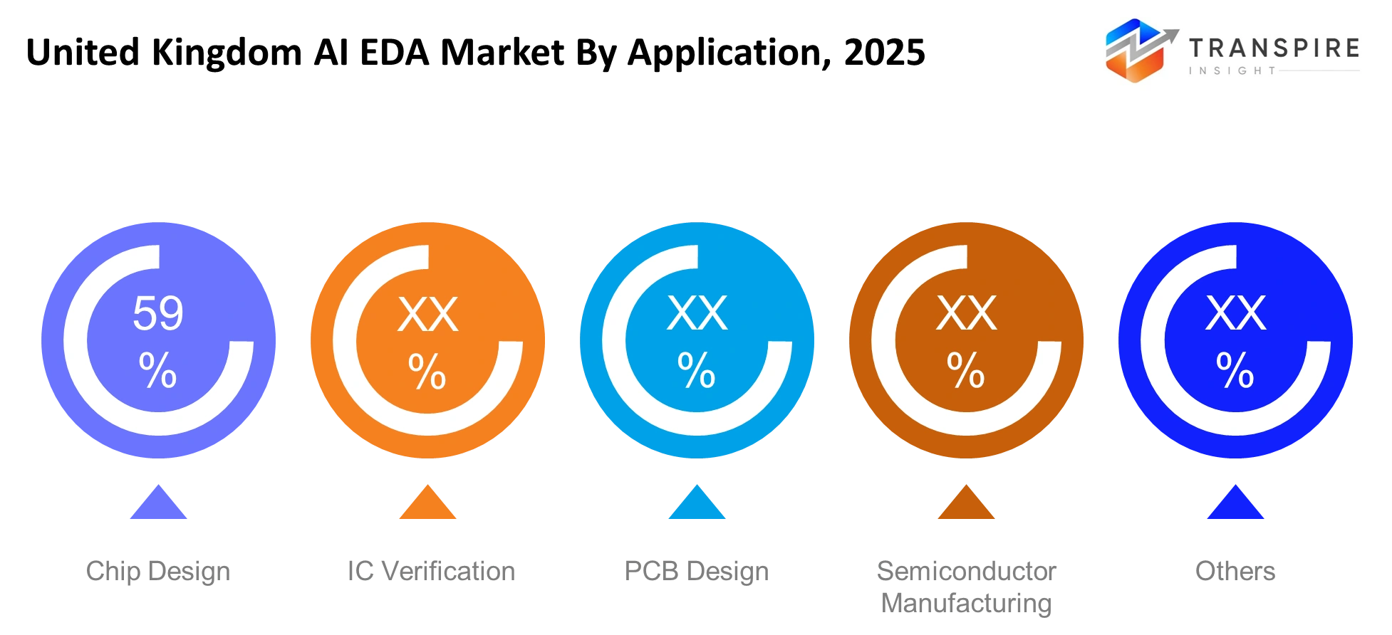
Chip design held the leading market spot, driven by expanding development work around AI processors , automotive electronics and high-performance computing semiconductors. Semiconductor companies also increased spending on AI-assisted design automation after earlier global chip shortages showed how costly delays can be, and how weak production flexibility becomes.IC verification kind of showed up as another big application space, since modern semiconductor blueprints really need a lot more verification steps across newer process nodes and these mixed, heterogeneous packaging configurations.
On the semiconductor manufacturing side, use cases are expected to keep rising pretty fast, mainly because predictive analytics tools are getting better at tuning yield and, in the same breath, trimming fabrication waste. AI-driven simulation environments increasingly help with defect forecasting, thermal management scrutiny, and even process calibration while wafers are in production. Meanwhile, PCB design applications also grew at a steady pace, because smaller electronics and edge computing gadgets pushed the need for tighter circuit layouts, plus faster design sprints. In the longer run, growth across all these segments should motivate software providers to build very tuned AI models for automotive, telecom, and defense semiconductor needs.
To learn more about this report, Download Free Sample Report
By Deployment
On-premise deployment stayed in the lead, as big semiconductor manufacturers focused heavily on intellectual property safeguards, low-latency processing, and having direct control over very sensitive chip design information. A lot of the advanced semiconductor programs kept leaning on in house compute infrastructure to run complicated simulations and protect confidential engineering workflows. Hybrid setups got a stronger share among mid sized design teams that wanted scalable compute power, without fully shifting the most critical workloads out to external cloud spaces.
Cloud based deployment kind of went up fast after 2021, mainly because distributed engineering groups and university-led semiconductor collaborations kept expanding all over the United Kingdom. The cloud native EDA setups got better at using resources properly, they helped teams collaborate in near real time, and they also cut down on infrastructure costs, especially for startup firms and fabless semiconductor organizations. During the forecast span, hybrid plus cloud deployment models are expected to pull in more investment , mostly tied to the rising need for adaptable simulation capacity and AI driven workflow automation. Buyers are also leaning more toward subscription style software ecosystems, ones that can support scale up computing performance and shorten product delivery timelines
By End User
Semiconductor companies were the biggest end-user group. This is because building advanced chips requires extensive verification, simulation, and design automation, not just one or two steps. At the same time, AI-focused semiconductor initiatives running in data centers, telecommunications, and automotive electronics increased the software budget for both integrated device manufacturers and fabless chip developers. Electronics manufacturers stayed involved too, since consumer devices and industrial automation systems demanded smaller and more power-efficient semiconductor components
Research institutes showed up as a pretty strategic growth segment. They benefited from growing government backed semiconductor innovation initiatives, plus university partnerships that kept strengthening the pipeline. For example, research clusters in Cambridge, and Scotland boosted the adoption of AI-enabled design platforms for photonics, compound semiconductors, and newer processor architectures. Over the forecast period, collaboration between academic institutions and commercial chip developers is expected to speed up demand for cloud based simulation tools and AI assisted verification systems. Investors plus software vendors are more and more aiming at research-driven semiconductor ecosystems, because early-stage innovation programs often help set future, commercial chip design standards.
What are the Key Use Cases Driving the United Kingdom AI EDA Market?
AI-assisted chip design still seems to be, like, the main use case pushing adoption all through the United Kingdom semiconductor scene. Basically, semiconductor businesses are leaning on AI EDA platforms to automate layout tuning, timing checks, and verification loops for advanced processors used in data centers, cars, and 5G backbone gear. That kind of application draws the most attention because today’s AI chips pack billions of transistors, so they need faster validation and lower power budgets.
IC verification plus PCB design tools are starting to pick up speed, too, especially among electronics manufacturers and telecom hardware suppliers. In the automotive world, companies building ADAS platforms increasingly turn to AI-driven simulation to reduce hardware mishaps and speed up the certification schedules. Even research institutes have been expanding usage, mostly for photonics and compound semiconductor development programs , kind of as a side effect of everything moving faster.
More new stuff is showing up as well, like generative AI-based analogue chip design and AI thermal optimisation for quantum computing machinery. Defense and aerospace efforts are also looking into autonomous verification systems for hardened processor architectures and reliability testing that matters for missions , not just benchmarks.
|
Report Metrics |
Details |
|
Market size value in 2025 |
USD 92.57 Million |
|
Market size value in 2026 |
USD 111.77 Million |
|
Revenue forecast in 2033 |
USD 418.14 Million |
|
Growth rate |
CAGR of 20.74% from 2026 to 2033 |
|
Base year |
2025 |
|
Historical data |
2021 - 2024 |
|
Forecast period |
2026 - 2033 |
|
Report coverage |
Revenue forecast, competitive landscape, growth factors, and trends |
|
Regional scope |
United Kingdom |
|
Key company profiled |
Synopsys, Cadence Design Systems, Siemens EDA, Ansys, Keysight Tech===nologies, Altium, Zuken, Silvaco, eInfochips, Intel, NVIDIA, Arm Holdings, IBM, Samsung Electronics, Xilinx |
|
Customization scope |
Free report customization (country, regional & segment scope). Avail customized purchase options to meet your exact research needs. |
|
Report Segmentation |
By Component (Software Tools, AI Algorithms, Cloud Platforms, Verification Tools, Others); By Application (Chip Design, IC Verification, PCB Design, Semiconductor Manufacturing, Others); By Deployment (Cloud-based, On-premise, Hybrid Systems, Others); By End User (Semiconductor Companies, Electronics Manufacturers, Research Institutes, Others) |
Which Regions are Driving the United Kingdom AI EDA Market Growth?
England kinda leads the United Kingdom AI EDA Market, mainly because it has a more concentrated semiconductor research ecosystem, a fairly strong venture funding scene and yeah an already set up chip design infrastructure. Cities like Cambridge, London and the South East sort of hold a tight cluster of semiconductor startups, AI computing firms, plus university-led research programs that keep generating demand for advanced electronic design automation platforms. Also, government backed semiconductor efforts along with defense technology investments made adoption of AI assisted verification and simulation tools get a real boost after 2022, even if it was already in motion. And honestly, the large cloud computing presence, plus access to very specialized engineering talent keeps reinforcing Englands dominant position, across these advanced chip development programs.
Scotland shows up as the second-largest regional contributor, but the growth story there is a bit different from that in England. You see more of a stable and research-oriented market structure thanks to compound semiconductor manufacturing, photonics research, and those long-running industrial partnerships. There is also steady investment coming from academic institutions and public-private semiconductor initiatives, which helps vendors keep deploying software for the longer term rather than chasing rapid short cycle expansion. That kind of steadiness lets EDA vendors protect recurring software revenue streams from research labs, aerospace programs, and precision electronics manufacturers spread around the region.
Northern Ireland and Wales are now looking like the fastest growing regional markets. This is mostly tied to expanding semiconductor modernization efforts, and more capital flowing into specialized electronics manufacturing. Regional authorities, along with industrial development agencies, pushed harder on AI hardware innovation, especially in telecom backbone, defense electronics, and edge computing set ups. Over the last three years, fresh partnerships between nearby universities and semiconductor companies made it easier to get into cloud based design workspaces and AI powered simulation instruments. So yeah, all this momentum ends up sounding like a pretty nice opening for software vendors as well as investors who want earlier access to the semiconductor clusters forming between 2026 and 2033.
Who are the Key Players in the United Kingdom AI EDA Market and How Do They Compete?
The competitive landscape of the United Kingdom AI EDA Market is still pretty moderately consolidated, meaning only a few global software vendors kinda hold a large chunk of advanced semiconductor design workflows. Lately the competition has been leaning more toward AI-driven automation features, cloud based co-working tools, and anything that can cut verification cycles down for tough chip architectures. The established players keep defending their share by going deeper with integration across multiple semiconductor design stages, while smaller AI focused companies try to win on narrow use cases like analog chip tuning and photonics simulation. At this point, technological momentum seems to outweigh pure price competition, since semiconductor teams care a lot about faster tape-out timelines, more dependable predictive verification, and the availability of scalable compute infrastructure.
Synopsys improves its stance with AI assisted verification, plus generative design optimization platforms that reduce engineering workloads for advanced node programs. There’s a strong link between simulation, testing, and design software, and that link becomes a real workflow advantage for big chip makers building AI accelerators, and also for automotive processors. Cadence Design Systems tends to differentiate via cloud native EDA environments and machine learning digital twin functions, which help with power analysis and system-level modeling in practice. In addition, strategic collaborations with hyperscale computing providers have expanded remote simulation capacity, enabling distributed engineering teams across the United Kingdom to work with less friction.
Siemens EDA, on the other hand, puts emphasis on industrial scale verification and digital manufacturing alignment, so it often looks especially competitive in aerospace, defense, and industrial semiconductor programs. Advanced lifecycle management tools and system-level simulation capabilities enable Siemens EDA to support highly regulated chip development programs that require traceability and compliance validation. Arm Holdings leverages strong domestic semiconductor influence through processor IP ecosystems optimized for AI workloads, edge computing, and automotive electronics. Continued partnerships with research institutions and semiconductor startups strengthen access to emerging chip architectures and long-term innovation programs within the UK semiconductor ecosystem.
Company List
- Synopsys
- Cadence Design Systems
- Siemens EDA
- Ansys
- Keysight Technologies
- Altium
- Zuken
- Silvaco
- eInfochips
- Intel
- NVIDIA
- Arm Holdings
- IBM
- Samsung Electronics
- Xilinx
Recent Development News
In April 2026, Synopsys announced a partnership with TSMC to deliver AI-powered EDA flows and certified IP solutions for next-generation AI systems. The collaboration strengthened advanced 2nm and 3nm chip design capabilities, improving productivity for AI and high-performance computing semiconductor programs. https://investor.synopsys.com
In March 2026, Cadence Design Systems entered a strategic collaboration with NVIDIA to develop accelerated engineering solutions for agentic AI chip and system design. The partnership integrated Cadence design platforms with NVIDIA accelerated computing infrastructure, enabling faster autonomous semiconductor design workflows and improved simulation performance. https://www.cadence.com
What Strategic Insights Define the Future of the United Kingdom AI EDA Market?
The United Kingdom AI EDA Market is heading toward more autonomous semiconductor design places where generative AI, predictive simulation, and cloud native verification systems will start replacing the work heavy engineering routines pretty fast. The need for advanced AI processors, edge computing hardware, and energy efficient semiconductor architectures will keep pushing this shift along for the next five to seven years. Still, there is a quieter danger, the fact that the key EDA know-how is getting more and more concentrated in a small set of big international software vendors. If the industry leans too hard on that limited group, licensing fees could rise, interoperability could get messy or limited, and strategic weak spots may show up, especially for smaller chip makers and for domestic innovation programs.
An interesting opportunity might be AI led photonics plus compound semiconductor design platforms that are tied to research groups around Scotland and Cambridge. These approaches are becoming more relevant as telecom operators, defense contractors, and quantum computing teams look for faster ways and more energy frugal processing architectures. Market players should probably build partnerships with universities and cloud infrastructure providers, so they can get early access to specialized semiconductor datasets, talent pipelines, and next generation AI verification models, before competitive barriers harden further.
United Kingdom AI EDA Market Report Segmentation
By Component
- Software Tools
- AI Algorithms
- Cloud Platforms
- Verification Tools
- Others
By Application
- Chip Design
- IC Verification
- PCB Design
- Semiconductor Manufacturing
- Others
By Deployment
- Cloud-based
- On-premise
- Hybrid Systems
- Others
By End User
- Semiconductor Companies
- Electronics Manufacturers
- Research Institutes
- Others
Frequently Asked Questions
Find quick answers to common questions.
The expected United Kingdom AI EDA Market size is USD 418.14 Million in 2033.
Key segments for the United Kingdom AI EDA Market are By Component (Software Tools, AI Algorithms, Cloud Platforms, Verification Tools, Others); By Application (Chip Design, IC Verification, PCB Design, Semiconductor Manufacturing, Others); By Deployment (Cloud-based, On-premise, Hybrid Systems, Others); By End User (Semiconductor Companies, Electronics Manufacturers, Research Institutes, Others).
Major United Kingdom AI EDA Market players are Synopsys, Cadence Design Systems, Siemens EDA, Ansys, Keysight Technologies, Altium, Zuken, Silvaco, eInfochips, Intel, NVIDIA, Arm Holdings, IBM, Samsung Electronics, Xilinx.
The United Kingdom AI EDA Market size is USD 92.57 Million in 2025.
The United Kingdom AI EDA Market CAGR is 20.74% from 2026 to 2033.
- Synopsys
- Cadence Design Systems
- Siemens EDA
- Ansys
- Keysight Technologies
- Altium
- Zuken
- Silvaco
- eInfochips
- Intel
- NVIDIA
- Arm Holdings
- IBM
- Samsung Electronics
- Xilinx
Recently Published Reports
-
Apr 2026
Fiber Optic Faceplates Market
Fiber Optic Faceplates Market Size, Share & Analysis Report By Type (< 300 mm2, 300-350 mm2, and > 350 mm2, By Application (Night Vision, Holographic Imaging, Medical, and Others), and Geography (North America, Europe, Asia-Pacific, Middle East and Africa, South and Central America), 2021 - 2031
-
Apr 2026
High Temperature Superconductors Market
High Temperature Superconductors Market Size, Share & Analysis Report By Type (1G HTS, and 2G HTS), By Application (Power Cable, Fault Current Limiter, and Transformer), and Geography (North America, Europe, Asia-Pacific, Middle East and Africa, South and Central America), 2021 - 2031
-
Apr 2026
Industrial Plugs and Socket Market
Industrial Plugs and Socket Market Size, Share & Analysis Report By Type (Industrial Plugs, Industrial Sockets), By Current (Up to 32 A, 32 to 125 A, Above 125 A), By Protection (Dustproof and Splash Proof, Waterproof, Explosion Proof), By End User (Heavy Industries, Oil and Gas, Chemicals and Pharmaceuticals, Power Generation, Others), and Geography (North America, Europe, Asia-Pacific, Middle East and Africa, South and Central America), 2021 - 2031
-
Apr 2026
InGaAs Avalanche Photodiodes Market
InGaAs Avalanche Photodiodes Market Size, Share & Analysis Report By Type (1100 - 1700 nm, and 1000 - 1600 nm), By Application (Missile Warning System, Muzzle Flash Detection, Wafer Defect Inspection, Laser Rangefinders, and Others), and Geography (North America, Europe, Asia-Pacific, Middle East and Africa, South and Central America), 2021 - 2031