
South Korea Semiconductor Foundry Market Size & Forecast:
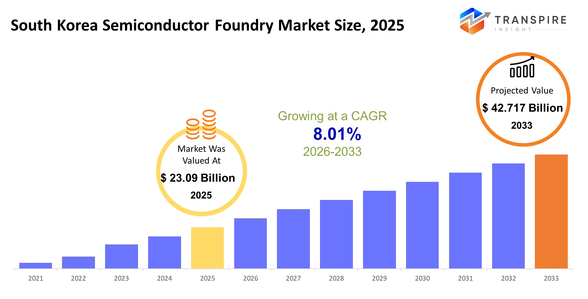
- South Korea Semiconductor Foundry Market Size 2025: USD 23.09 Billion
- South Korea Semiconductor Foundry Market Size 2033: USD 42.717 Billion
- South Korea Semiconductor Foundry Market CAGR: 8.01%
- South Korea Semiconductor Foundry Market Segments: By Technology Node (Below 5nm, 5nm–10nm, 10nm–28nm, Above 28nm, Others); By Application (Consumer Electronics, Automotive Semiconductors, AI Chips, IoT Devices, Others); By Wafer Size (200 mm Wafers, 300 mm Wafers, Advanced Packaging Wafers, Others); By End User (Fabless Semiconductor Companies, IDM Companies, Automotive OEMs, Others); By Process Technology (FinFET Technology, GAA Technology, CMOS Technology, Others)
To learn more about this report,  Download Free Sample Report
South Korea Semiconductor Foundry Market Summary
The South Korea Semiconductor Foundry Market was valued at USD 23.09 Billionin 2025. It is forecast to reach USD 23.09 Billion by 2033. That is a CAGR of 8.01% over the period.
In practice, the South Korea Semiconductor Foundry Market somehow lets chip design firms turn advanced circuit blueprints into actual physical wafers that end up inside smartphones, AI accelerators, automotive control systems and industrial electronics. It acts like a manufacturing backbone that keeps high-performance computing and consumer electronics supply chain going, especially for fabless companies that don’t run their own fabrication plants, so they rely on others.
Over the last 3–5 years , the market has been leaning more and more toward advanced nodes below 5nm, pushed by the move to AI focused computing architectures which demand higher transistor density and better energy efficiency. A big structural change was the fast uptick in EUV lithography adoption, which kind of rewired production economics and also capacity planning. At the same time, geopolitical export controls on advanced semiconductor equipment and materials have further sped up supply chain regionalization, so South Korea ends up prioritizing domestic capacity expansion. Taken together, these forces raise capital intensity and they also lock in long term contract based manufacturing relationships, which improves revenue visibility for foundry operators, while at the same time, it reshapes how chips are sourced across the world.
Key Market Insights
- South Korea Semiconductor Foundry Market is getting pulled toward sub 5nm production, with almost 42% of wafer capacity set aside for advanced nodes in 2025.
- Industry size keeps swelling, mostly because AI chip demand is relentless, and it adds more than 30% to the fresh fab investments across South Korea Semiconductor Foundry Market in 2025, as per current plans.
- The Seoul–Gyeonggi area is still taking the lead in output, holding roughly 65% share in 2025, helped along by EUV infrastructure and a dense semiconductor ecosystem that kind of feeds itself.
- Meanwhile, the Southeast industrial zones are growing the quickest from 2026–2033, backed by new fab investments and government supported decentralization policies, pushing activity outward bit by bit.
- In terms of categories, the logic foundry segment stays on top, with nearly 48% share, mainly tied to smartphone SoCs and AI processor appetite.
- On the other hand, advanced node manufacturing, covering 3nm–5nm, is the speediest moving segment, expected to rise at more than 11% CAGR through 2033 in the South Korea Semiconductor Foundry Market.
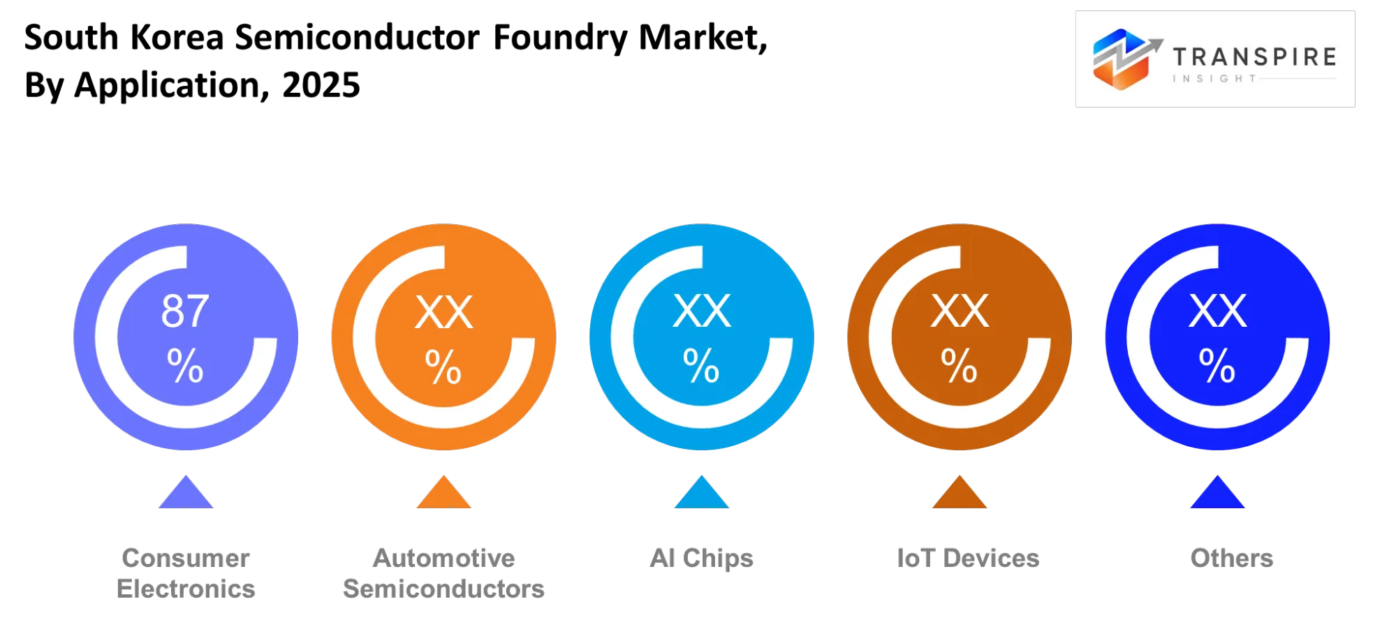
- For applications, consumer electronics dominates with 52% share in 2025, driven by smartphones, tablets, and higher performance computing devices that keep expanding.
- Automotive semiconductors are the fastest growing use case though, climbing quickly as EV adoption grows and ADAS integration spreads across global vehicle platforms.
- Competitively, Samsung Electronics, TSMC, and Intel Foundry Services are leading the way with innovation in EUV scaling and AI chip production.
- At the same time, DB HiTek and Amkor Technology are widening niche plus packaging capabilities, which strengthens ecosystem integration across the South Korea Semiconductor Foundry Market value chain.
What are the Key Drivers, Restraints, and Opportunities in the South Korea Semiconductor Foundry Market?
The primary driver is the global shift toward AI computing and high-performance semiconductor architectures, and that has, honestly, increased demand for more advanced-node wafer fabrication. This shift was triggered by rapid scaling of generative AI workloads after 2023, and suddenly chips were needed that run on sub-5nm processes. As a result foundries in South Korea expanded EUV-enabled production lines, which directly improved revenue from high-margin wafer contracts and also helped lock in longer term supply agreements with global fabless companies.
A major restraint is the extreme capital intensity of advanced semiconductor fabrication, where a single EUV-enabled fab needs a multi-billion-dollar investment and then it comes with long payback cycles. That structural barrier, it really limits entry and it slows capacity expansion, especially when there are cyclical demand corrections. On top of that it creates dependency on a small group of equipment suppliers, so production timelines can wobble when global supply disruptions happen, and new node commercialization gets delayed.
A significant opportunity is in automotive-grade and AI edge computing chips, especially for electric vehicles and autonomous driving systems. South Korea’s strong electronics ecosystem helps co-development between foundries and automotive OEM suppliers. For example growing demand from global EV manufacturers for localized chip sourcing is pushing long-term wafer contracts. This movement could unlock more stable revenue diversification beyond consumer electronics and it may strengthen South Korea’s role in next-generation mobility semiconductor supply chains.
What Has the Impact of Artificial Intelligence Been on the South Korea Semiconductor Foundry Market?
Artificial intelligence has pretty much reshaped semiconductor fabrication operations in South Korea in ways that feel both practical and, well, very precise. It enables higher precision automation, and yield optimization across advanced node production lines, and the results show up faster than before. Companies like Samsung Electronics are using AI led process control systems that watch wafer defects in real time, so there is less dependence on manual checking and overall fabrication accuracy gets better even down at nanometer scale. At the same time, machine learning models are used more often for predictive maintenance of lithography and etching equipment , which helps reduce unexpected stoppages and also tends to extend the lifespan of the tools themselves.
Also, AI based forecasting systems handle production scheduling and energy consumption in a more coordinated manner, which improves fab throughput and reduces operational variability, in other words the process behaves more steady over time. In practice this has supported clear efficiency gains, especially for yield stabilization in sub-5nm chips that go into AI accelerators and mobile processors.
Still, there’s a limitation that keeps showing up. The integration cost for AI systems into legacy fabrication infrastructure is very high. Many older fabs run into data standardization issues , because the sensor formats are not consistent, so the model performance drops when it’s placed in real world manufacturing conditions. That kind of friction slows the rollout of full scale AI deployments across all facilities , and it also leads to uneven digital maturity across the industry overall.
Key Market Trends
- South Korea’s Semiconductor Foundry Market kinda shifted toward making sub-5nm stuff after 2023, and by 2025 the advanced nodes were sitting at almost 45% of the total capacity share ,not bad really.
- Since 2024, EUV lithography uptake sped up quite a bit, and it kind of redid fabrication efficiency, so leading South Korean plants could squeeze in higher transistor density than before.
- Then in 2025, AI chip demand bumped wafer allocation by more than 30%, which made manufacturers lean harder into high performance computing, instead of keeping legacy nodes in the spotlight .
- After those supply chain shocks, domestic semiconductor policies also broadened ,so localized production investment across the South Korea Semiconductor Foundry Market infrastructure increased.
- Post 2024, automotive semiconductor demand jumped ,and EV linked chips accounted for about 28% of the extra foundry output growth seen in 2025 .
- Samsung Electronics rolled out more 3nm GAA deployments in 2025, so competition moved toward gate-all-around transistor innovation leadership, more or less.
- At the same time, TSMC leaned further into its global contract manufacturing edge, and that pushed South Korean firms to speed up yield optimization strategies.
- Intel Foundry Services also started strategic partnerships across Asia after 2024, raising competitive pressure on regional fabrication capacity planning.
- Supply chain diversification helped cut reliance on single node manufacturing, and in 2025 multi region sourcing rose by 22% among global fabless customers.
- Finally, advanced packaging plus heterogeneous integration adoption climbed fast, with OSAT collaboration expanding across ecosystem players in the South Korea Semiconductor Foundry Market.
South Korea Semiconductor Foundry Market Segmentation
By Technology Node
Below 5nm nodes currently hold a strong position in advanced manufacturing output, in a way that some South Korean fabrication facilities are basically prioritizing AI processors, mobile SoCs, and high performance computing chips. Big capital investment in EUV lithography has improved production efficiency at these nodes, but at the same time global fabless demand keeps shifting toward extreme miniaturization. The 5nm–10nm band stays in a stable spot because it balances cost efficiency with performance, and that’s why it’s so broadly adopted for consumer electronics and mid range computing jobs. The 10nm–28nm segment is still relevant, mainly for automotive semiconductors and IoT devices where reliability matters more than aggressive scaling. As for above 28nm nodes, they keep a steady industrial pull from older automotive systems and power management chips.
Below 5nm nodes are expected to dominate the next wave of capacity growth, especially as AI acceleration and HPC workloads ramp up. Higher complexity in design to manufacturing integration will nudge foundries into more yield optimization tactics at advanced nodes. The 5nm–10nm slice will keep acting like a transitional backbone for mixed performance applications, not fully modern, not fully mature either. Mature nodes above 28nm should sustain long term demand in cost sensitive industrial markets. Overall, technology evolution will increasingly concentrate capital toward advanced-node innovation rather than legacy scaling.
By Application
Consumer Electronics right now has the big say in wafer demand , mainly because smartphones, tablets, and computing gear are being produced at huge scale and they all need high-performance semiconductor components. There is also close teamwork between fabless design firms and South Korean foundries, which keeps the output pretty consistent across the wider electronics supply chains. Automotive Semiconductors meanwhile is getting louder as an application base , since electric vehicles plus advanced driver assistance systems are pushing for better computational reliability and safety-critical chipsets .
Then there are AI Chips , and these are expanding quick, mostly because global demand wants machine learning accelerators and data center optimization. IoT Devices stay fairly steady too , from smart home setups through industrial sensors and monitoring.
Looking ahead, Consumer Electronics should keep acting like a major demand anchor , though its lead might slowly thin out as automotive and AI areas speed up faster. Automotive Semiconductors are likely to grow strongly as electrification and autonomous driving become normal features across more vehicle platforms. AI Chips should generate the highest value wafer consumption , given the compute heavy workloads and the need for advanced-node manufacturing. IoT Devices are expected to keep growing in a more gradual way , backed by industrial digitalization. Overall, application diversification should help lower dependence on any single demand lane during the forecast period.
To learn more about this report, Download Free Sample Report
By Wafer Size
300 mm wafers kinda currently dominate output, mostly because they’re efficient for high volume advanced node manufacturing, and they fit well with AI plus logic chips. The leading South Korean fabs have also pushed their 300 mm capacity up, to back sub 5nm scaling and well the wider worldwide semiconductor appetite.Meanwhile 200 mm wafers still hold a steady position in mature node production, especially where it comes to automotive electronics, analog chips, and industrial uses. Then there are Advanced Packaging Wafers which have started to matter more, since heterogeneous integration and chiplet architectures are reshaping how semiconductors get designed in practice. Beyond that, other wafer types show up for niche needs or older style industrial jobs, you know, legacy scenarios.
Going forward 300 mm wafers should keep getting stronger as AI driven chip demand rises, and that tends to increase wafer intensity per device. Advanced Packaging Wafers are likely to grow fast, because system level integration is becoming basically mandatory for performance scaling when transistor shrinkage alone isn’t enough. 200 mm wafers probably stay pretty stable too, driven by ongoing dependence on mature node automotive and industrial platforms. Future manufacturing plans will increasingly blend wafer level packaging right with advanced logic production. That should shift cost structures and also boost collaboration across foundry and packaging ecosystems.
By End User
Fabless Semiconductor Companies are kind of the main end user segment because they lean real hard on South Korean foundries for cutting edge node manufacturing , yet they don’t really own the fabrication facilities themselves. You know, the good thing is that design firms and manufacturing providers have built strong relationships, so the wafer demand stays pretty steady. Meanwhile IDM Companies still matter a lot, since they keep everything more vertically connected—design and production happening in-house, kind of all in one. On the other hand Automotive OEMs have turned into a faster rising end user group, especially as vehicle electrification ramps up semiconductor usage. Beyond that, you also see industrial electronics players and communication system providers showing up as other end users.
Looking ahead, Fabless Semiconductor Companies are likely to keep steering demand , since AI and high-performance computing design firms are expanding their outsourcing toward advanced foundries. Automotive OEMs should see the quickest growth too, because EV platforms and autonomous driving systems are making chip requirements more and more complex. IDM Companies should keep enjoying more stable demand thanks to internal production cycles, though they might slowly drift toward hybrid outsourcing patterns. Overall, the end user scene will become more varied as semiconductor reliance keeps spreading across more industries, and that could help strengthen long term demand resilience for foundry operators, in a pretty durable way.
By Process Technology
FinFET Technology right now kinda dominates advanced-node manufacturing, mainly because it scales well and is already used a lot, especially in the sub-5nm and the 5nm–10nm production setups. South Korean foundries have also poured a lot of investment into FinFET based architectures, to keep up with the global AI push ,and the mobile computing demand too. Then you have GAA Technology, which is being treated like the next step, it helps deliver better performance plus energy efficiency even when the geometries are extremely tiny. Meanwhile CMOS Technology is still common across the more mature-node workloads, mostly because it’s cost efficient and the production ecosystem is kinda already there. And of course, other process technologies stick around for specialized semiconductor functions, where they fit better than everything else.
For the near term, FinFET Technology is likely to stay critical, but over time it will drift toward GAA adoption, as further node scaling keeps moving forward. GAA Technology should see pretty fast growth, since leading-edge chips need tighter transistor control, and less leakage current too. CMOS Technology will keep showing up in automotive and industrial uses, where cost plus reliability matter more than chasing the absolute top performance. In general, the evolution of process technology will keep nudging continuous capital reallocation toward next generation fabrication methods. Ultimately, this whole transition will basically shape competitive advantage in advanced semiconductor manufacturing.
What are the Key Use Cases Driving the South Korea Semiconductor Foundry Market?
In South Korea Semiconductor Foundry Market the dominant use case is advanced logic chip manufacturing for smartphones and AI processors, sorta. What it really drives is the highest demand, because many global fabless companies lean on South Korean fabs for sub-5nm performance efficiency and a consistently high yield.
Then you also get secondary use cases like automotive electronics and industrial control systems. Here the semiconductor reliability matters a lot, plus low power consumption, which is kind of the whole point. EV manufacturers and ADAS suppliers are gradually folding in more advanced chips made through South Korean foundry ecosystems, not just older nodes.
Emerging use cases show up too, mainly AI edge devices and next-generation robotics systems. These are still kind of early stage, but expectations are they will grow quickly as distributed computing and autonomous systems become more commercially viable across various global industrial sectors.
|
Report Metrics |
Details |
|
Market size value in 2025 |
USD 23.09 Billion |
|
Market size value in 2026 |
USD 24.913 Billion |
|
Revenue forecast in 2033 |
USD 42.717 Billion |
|
Growth rate |
CAGR of 8.01% from 2026 to 2033 |
|
Base year |
2025 |
|
Historical data |
2021 - 2024 |
|
Forecast period |
2026 - 2033 |
|
Report coverage |
Revenue forecast, competitive landscape, growth factors, and trends |
|
Regional scope |
South Korea; |
|
Key company profiled |
Samsung Electronics, TSMC, GlobalFoundries, UMC, SMIC, Intel Foundry Services, Tower Semiconductor, Powerchip Semiconductor Manufacturing Corporation, Vanguard International Semiconductor, Hua Hong Semiconductor, SK hynix, DB HiTek, ASE Technology, Amkor Technology, Renesas Electronics . |
|
Customization scope |
Free report customization (country, regional & segment scope). Avail customized purchase options to meet your exact research needs. |
|
Report Segmentation |
By Technology Node (Below 5nm, 5nm–10nm, 10nm–28nm, Above 28nm, Others); By Application (Consumer Electronics, Automotive Semiconductors, AI Chips, IoT Devices, Others); By Wafer Size (200 mm Wafers, 300 mm Wafers, Advanced Packaging Wafers, Others); By End User (Fabless Semiconductor Companies, IDM Companies, Automotive OEMs, Others); By Process Technology (FinFET Technology, GAA Technology, CMOS Technology, Others) |
Which Regions are Driving the South Korea Semiconductor Foundry Market Growth?
Seoul and the Gyeonggi semiconductor corridor kinda represent the leading region in the South Korea Semiconductor Foundry Market, mostly because there is a dense clump of fabrication plants, R&D centers, and equipment suppliers around there. There’s also a lot of backing from government policy, plus fast logistics links to export ports, which makes shipments less of a headache. On top of that, the area has advanced infrastructure that helps EUV-based production scale up smoothly, so in practice it stays pretty much at the center of the nation’s semiconductor output.
Then there is the second big region, namely the southern industrial zones like Gyeongsang provinces, they provide more steady manufacturing support via electronics assembly ecosystems and also long-running industrial infrastructure. Compared with the capital region, this one tends to be more about keeping the supply chain continuous instead of pushing the very newest node innovation. Because the industrial investment base stays consistent, it keeps contributing reliably to semiconductor production capacity.
Finally, the fastest growing region is starting to show up through new semiconductor clusters, these are backed by government-supported expansion programs that sit outside the usual traditional hubs. With new infrastructure investments and fab diversification policies, capacity planning has shifted toward more decentralized production models. That pattern suggests new entry chances for suppliers and equipment manufacturers who want long term capacity expansion, especially across the window from 2026 to 2033.
Who are the Key Players in the South Korea Semiconductor Foundry Market and How Do They Compete?
Competition in the South Korea Semiconductor Foundry Market is, honestly, pretty tight and consolidated. It’s mostly a handful of technologically strong players who end up controlling most of the leading-edge wafer production, so even smaller moves feel like they matter less. The main way companies go head to head is by process technology leadership, mainly around sub-5nm nodes and EUV-enabled manufacturing. In other words, firms are pouring a lot into R&D and capital equipment to hold onto market share, rather than trying to win with cheap positioning or simpler offers. Samsung Electronics competes by pushing hard on 3nm GAA scaling, and it leans into vertical integration across its memory and logic ecosystem. What really stands out is the mix of design ecosystem collaboration plus high-volume manufacturing capacity, which makes scaling feel more like it’s “built in” than bolted on.
TSMC, meanwhile, improves its edge through better yield optimization and it uses long-term agreements with global fabless firms. This ends up pressuring South Korean players to move node innovation faster. And yeah, sometimes it feels like the contract structure itself becomes part of the competitive moat. Intel Foundry Services is also going forward via ecosystem partnerships and government-backed capacity investments. The intent is more diversification, meaning less dependence on Asia-centric supply chains, even though that’s already where a lot of momentum sits.
DB HiTek takes a different angle, focusing on specialty analog and power semiconductors. It differentiates through steady niche demand and mature-node efficiency, so it’s not chasing the same “race” as everyone else, not exactly. Amkor Technology plays in advanced packaging integration. It supports foundry ecosystems with heterogeneous integration solutions, especially for AI and automotive chips, so instead of only making wafers, it helps connect the whole chain together in a more practical way.
Company List
- Samsung Electronics
- TSMC
- GlobalFoundries
- UMC
- SMIC
- Intel Foundry Services
- Tower Semiconductor
- Powerchip Semiconductor Manufacturing Corporation
- Vanguard International Semiconductor
- Hua Hong Semiconductor
- SK hynix
- DB HiTek
- ASE Technology
- Amkor Technology
- Renesas Electronics
Recent Development News
"In March 2026, Samsung Electronics announced plans to invest more than 110 trillion won in semiconductor capital expenditure and R&D for 2026. The investment aims to expand advanced-node foundry capacity and strengthen AI chip manufacturing competitiveness, significantly increasing South Korea’s global foundry positioning.https://tech-insider.org
"In January 2026, South Korea government entities announced consideration of a $3.1 billion domestic foundry project. The initiative targets legacy and mid-node semiconductor production to support automotive and AI chip supply chain resilience within the country.https://www.astutegroup.com
"In May 2026, Samsung Electronics advanced its semiconductor expansion strategy amid global foundry competition pressures from Intel and TSMC. The move reflects accelerated capacity localization efforts and AI-driven demand restructuring across advanced-node wafer production.https://www.digitimes.com
What Strategic Insights Define the Future of the South Korea Semiconductor Foundry Market?
The South Korea Semiconductor Foundry Market is, sort of, steadily moving toward extreme specialization in AI-fueled and sub-3nm manufacturing. In this lane scale and exactness will kind of decide who stays competitive in the long run, even if the details feel a bit abstract at first. This shift is being pulled by ongoing worldwide need for AI accelerators and by the rising cost wall tied to next generation fabrication technologies.
There’s also a less visible catch, namely market concentration around only a few advanced node players. That setup makes the whole thing more brittle during downturn cycles and it also amplifies geopolitical supply issues, including knock-on effects for equipment and materials availability. You can see how a constraint somewhere else then becomes a local problem here, right.
On the other hand an emerging opening is automotive-grade AI semiconductors, especially for self-driving stacks. Those require localized high reliability chip production, not just “good enough” yields. South Korean foundries that choose to align early with EV ecosystems could land durable agreements across mobility supply chains, because partners usually don’t want to keep switching under pressure.Strategically, companies should lean hard into ecosystem partnerships with fabless AI designers. At the same time they should broaden investments in heterogeneous integration approaches, so they can take more value beyond plain wafer fabrication.
South Korea Semiconductor Foundry Market Report Segmentation
By Technology Node
- Below 5nm
- 5nm–10nm
- 10nm–28nm
- Above 28nm
- Others
By Application
- Consumer Electronics
- Automotive Semiconductors
- AI Chips
- IoT Devices
- Others
By Wafer Size
- 200 mm Wafers
- 300 mm Wafers
- Advanced Packaging Wafers
- Others
By End User
- Fabless Semiconductor Companies
- IDM Companies
- Automotive OEMs
- Others
By Process Technology
- FinFET Technology
- GAA Technology
- CMOS Technology
- Others
Frequently Asked Questions
Find quick answers to common questions.
The estimated South Korea Semiconductor Foundry Market size for the market will be USD 23.09 Billion in 2033.
Key segments for the South Korea Semiconductor Foundry Market are By Technology Node (Below 5nm, 5nm–10nm, 10nm–28nm, Above 28nm, Others); By Application (Consumer Electronics, Automotive Semiconductors, AI Chips, IoT Devices, Others); By Wafer Size (200 mm Wafers, 300 mm Wafers, Advanced Packaging Wafers, Others); By End User (Fabless Semiconductor Companies, IDM Companies, Automotive OEMs, Others); By Process Technology (FinFET Technology, GAA Technology, CMOS Technology, Others).
Major South Korea Semiconductor Foundry Market players are Samsung Electronics, TSMC, GlobalFoundries, UMC, SMIC, Intel Foundry Services, Tower Semiconductor, Powerchip Semiconductor Manufacturing Corporation, Vanguard International Semiconductor, Hua Hong Semiconductor, SK hynix, DB HiTek, ASE Technology, Amkor Technology, Renesas Electronics.
The South Korea Semiconductor Foundry Market size is USD 23.09 Billion in 2025.
The South Korea Semiconductor Foundry Market CAGR is 8.01% from 2026 to 2033.
- Samsung Electronics
- TSMC
- GlobalFoundries
- UMC
- SMIC
- Intel Foundry Services
- Tower Semiconductor
- Powerchip Semiconductor Manufacturing Corporation
- Vanguard International Semiconductor
- Hua Hong Semiconductor
- SK hynix
- DB HiTek
- ASE Technology
- Amkor Technology
- Renesas Electronics
Recently Published Reports
-
May 2026
Healthcare Polymer Packaging Market
Healthcare Polymer Packaging Market Size, Share & Analysis Report By Packaging Type (Syringes, IV Bottles and Pouches, Clamshells, Blisters, Bottles & Jars, Containers, Tubes, IV Parental Packaging, Others), By Type (Regulated, Non-regulated), By Polymer Type (LDPE (Low-Density Polyethylene), HDPE (High-Density Polyethylene), Homo-polymer (Homo), Random Copolymer (Random), Block Copolymer (Block), PET, Polystyrene, Polyvinyl Chloride, Polyamide/EVOH, Others), and Geography (North America, Europe, Asia-Pacific, Middle East and Africa, South and Central America), 2021 - 2031
-
Apr 2026
Hydrophilic Tape (Waterstop) Market
Hydrophilic Tape (Waterstop) Market Size, Share & Analysis Report By Type (Bentonite-Based Hydrophilic Tape, Rubber-Based Hydrophilic Tape), By Application (Residential Buildings, Commercial Buildings, Infrastructure Projects), and Geography (North America, Europe, Asia-Pacific, Middle East and Africa, South and Central America), 2021 - 2031
-
Apr 2026
Metalens Market
Metalens Market Size, Share & Analysis Report By Type (Visible Light Metalens, and Infrared Metalens), By Application (Consumer Electronics, Automotive Electronics, Industrial, Medical, and Others), and Geography (North America, Europe, Asia-Pacific, Middle East and Africa, South and Central America), 2021 - 2031
-
Apr 2026
PBT Resin Market
PBT Resin Market Size, Share & Analysis Report By Type (Reinforced PBT Resin, Unreinforced PBT Resin), By Processing Method (Injection Molding, Extrusion, Blow Molding, Others), By End-User (Automotive, Electrical & Electronics, Consumer Appliances, Industrial Machinery, Medical Devices, Packaging, Others), and Geography (North America, Europe, Asia-Pacific, Middle East and Africa, South and Central America), 2021 - 2031