
Semiconductor Silicon Wafer Market Summary:
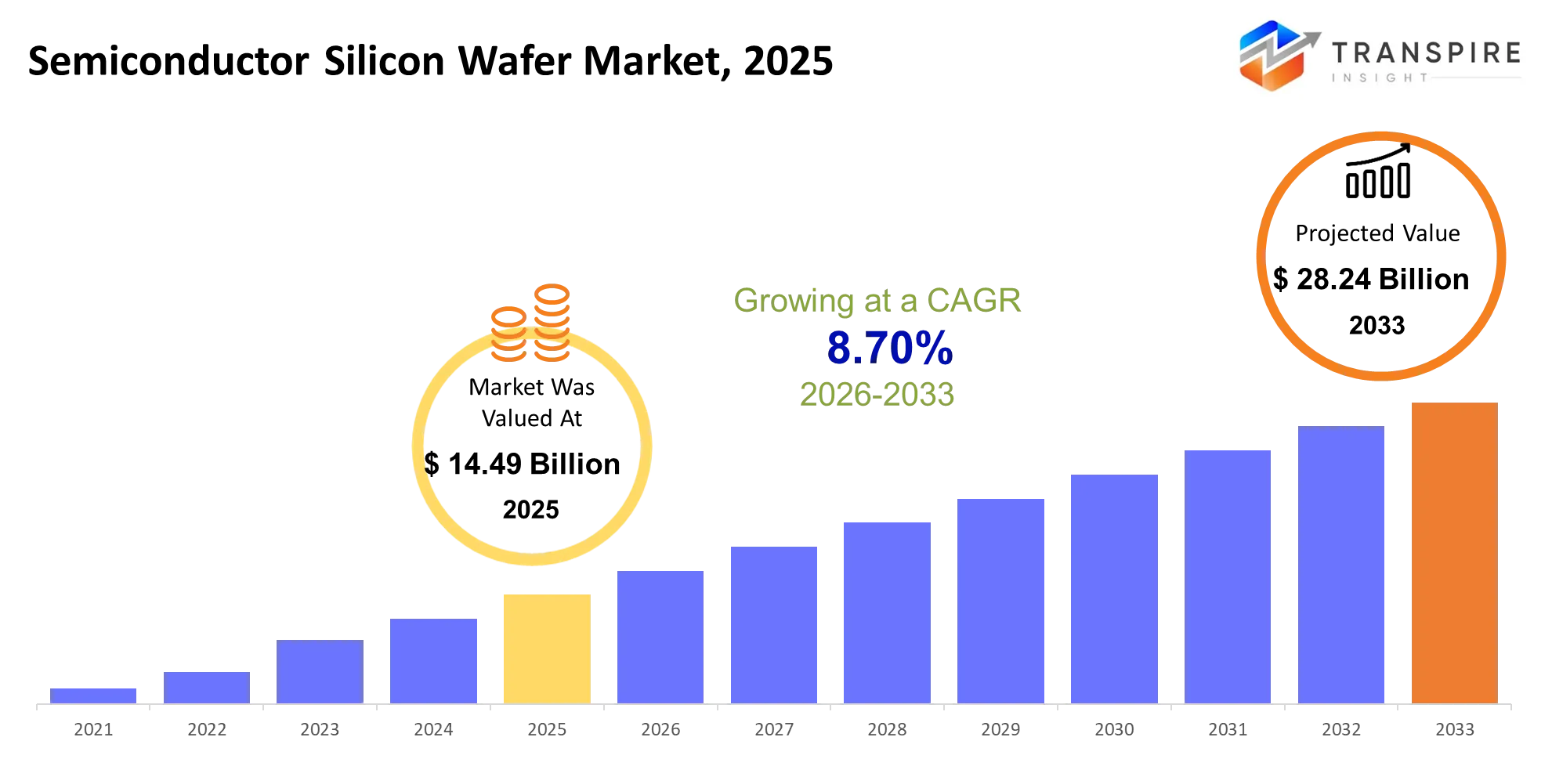
As per the Transpire Insight, The Semiconductor Silicon Wafer Market size is estimated at USD 14.49 billion in 2025 and is expected to reach USD 28.24 billion by 2033, growing at a CAGR of 8.70% from 2026 to 2033.
The semiconductor silicon wafer market is the host substrate on which chips, memory, sensors, power, and photonics are fabricated. Trends for purchasing have moved in the last three to five years from volume economics to diameter, purity, flatness, speciality layers, and assured regional supply. This structural change is toward 300mm for advanced logic and memory, while the infrastructure for AI is driving wafer demand in power-management and photonics devices. A relevant real-world driver for the current period is the AI data centre build-out, which is sustaining advanced logic and memory wafer demand and investment in 300mm fabrication facilities, as well as bolstering commitments to wafer supply. SEMI estimated that wafer shipment volume grew 7.4% year-on-year in Q2 2026, driven by AI demand in applications beyond advanced logic and memory. Additionally, regional semiconductor incentives and supply chain diversification are supporting local capacity and growing higher-end semiconductor manufacturing to overcome the costs of fab expansion as well as a shift to more complex nodes.
Semiconductor Silicon Wafer Market Size & Forecast:
- Market Size 2025: USD 14.49 Billion
- Expected Market Value (2033): USD 28.24 Billion
- Forecast CAGR (2026-2033): 8.70%
- Leading Region in 2025: Asia Pacific
- Fastest Growing Region: North America
- Key Company Profiles: Shin-Etsu Chemical, SUMCO, GlobalWafers, Siltronic, SK Siltron, Soitec, Wafer Works, Okmetic, Simgui, Siltronix Silicon Technologies, Virginia Semiconductor, Episil, Ferrotec, GRINM Semiconductor Materials, Mimasu Semiconductor Industry.
Key Semiconductor Silicon Wafer Market Insights:
The silicon wafer market is converging on 300mm advanced substrates for AI and HBM, with Japanese and Taiwanese players gaining a tighter grip on the supply of prime-grade wafers. Strategic capex is transitioning from general 2nm/3nm-ready capacity to regional hubs, with CHIPS incentives.
- Shin-Etsu and SUMCO are jointly responsible for ~50% of the wafer market share and 85% of 300mm capacity, with an investment of USD 1 billion in 2025 to bring 200,000 wafers/month to 2nm/3nm nodes.
- GlobalWafers is progressing the USD 7.5 billion U.S. plant in Sherman, Texas, with Phase 2 of its 300mm facility now operating to supply domestic foundries, launched in January 2026.
- In Korea, the 300mm prime capacity is dominated by SK Siltron, SUMCO and Shin-Etsu, which is a moderate-concentration supply base for memory and logic.
- A significant portion of SOI supply is controlled by Soitec and its partners, and as 300mm SOI pilots enter small-batch production, RF, power and silicon-photonics devices gain ground.
- Shanghai Silicon Industry is scaling up its 300mm capacity to 1.2 million wafers per month by the end of 2026 and launching a 300,000-wafer/year SOI pilot for EV and AI sensors.
- TSMC's Taiwan, the U.S., and Japan fab program, which will have ~1.2 million monthly 300mm starts in total, will provide wafer demand visibility.
- The automotive demand is driving 200mm wafers to 56.48% of the automotive wafer market in 2025, and 300mm wafers for automotive are growing at a 7.45% CAGR towards 2031.
- IDMs and foundries are entering into longer-term qualification and supply contracts for 300mm prime and epi wafers, as the top five merchant suppliers now account for the majority of volume.
What are the Key Drivers, Restraints, and Opportunities in the Semiconductor Silicon Wafer Market?
Driver:
The growth is driven by the rise of AI servers, the use of HBM, encouraging memory makers to migrate capacity from NAND to DRAM and HBM, and by generative AI training and inference workloads that accelerate shipment of GPUs/accelerators and amplify wafer demand per system. As a result, prime-grade 300mm wafer ASPs are rising, qualification queues are tightening, suppliers' utilisation is improving, and revenue resiliency is improving despite softer demand for consumer electronics.
Restraint:
Growth is limited by high capital intensity and long lead times for adding 300mm crystal-pulling and finishing capacity, while export controls can restrict equipment access. This persists because crystal-growth furnaces, ultra-high-purity polysilicon, and defect-control processes require lengthy qualification and precise process control. Rapid expansion can compromise yields, creating a structural capacity bottleneck for wafer suppliers.
Opportunity:
A future shift that can unlock growth is the expansion of domestic 300mm wafer capacity across India and Southeast Asia, supported by policy incentives, local anchor fabs, and supply-chain localization. Singapore provides a relevant example, with multi-billion-dollar semiconductor investments strengthening its manufacturing ecosystem and encouraging AI-enabled fab optimization. This model can support regional wafer production linked to advanced packaging, power devices, and specialty semiconductor applications. As local fabrication capacity expands, wafer suppliers can establish closer customer relationships, reduce logistics exposure, shorten qualification cycles, and create more resilient regional supply networks for advanced semiconductor manufacturing.
What Has the Impact of Artificial Intelligence Been on the Semiconductor Silicon Wafer Market?
AI is changing the silicon wafer market in many ways - affecting wafer volume and business priorities. The use of AI accelerators, high-bandwidth memory, and data-centre processors all require higher logic and memory capacity, which drives up 300mm-wafer volume. According to the Semiconductor Equipment and Materials International (SEMI), wafer shipment growth in the second quarter of 2026 rose 7.4% year-over-year as demand for AI began moving into power devices and photonics.
In wafer fabrication, AI and machine-learning tools can evaluate crystal-growth conditions, process signals, and metrology measurements to determine process windows, track drift, and reduce the amount of scrap. Models can be used to predict which equipment is more likely to experience anomalies ahead of time, helping to improve uptime and stabilize yields, while computer-vision inspection can be used to categorize surface defects and support stricter quality control, given more-demanding wafer specifications. The tools can also be used operationally to optimize scheduling, energy consumption, and chemical use when process conditions match production needs. AI applications require extensive high-quality data, devices integrated with legacy equipment, and specialist engineering knowledge. Errors in models or training data can lead to false positives, so validation by humans remains critical for high-value wafers.
In July 2026, Micron announced a strategic financing agreement to provide $500 million to GlobalWafers to expand 300mm raw silicon wafer production capacity. This funding directly supports the growing substrate requirements driven by artificial intelligence data centers and high-bandwidth memory expansion.
https://www.openpr.com/news/4602983/silicon-wafer-market-2026-accelerates-as-ai-chips-hbm-and-u-s
Key Semiconductor Silicon Wafer Market Trends:
The market is shifting from wafer-volume recovery to a selective mix driven by artificial intelligence infrastructure, advanced-node migration, regional supply policies, and substrate specifications.
- As the major logic and HBM memory technologies target big-diameter wafers, 300mm wafer share is growing to about three-quarters of shipped area.
- Advanced node and 3D stacking needs for AI accelerators and high-end SoCs are driving the growth of epitaxial 300mm wafers.
- Memory makers are transitioning capacity from NAND to DRAM/HBM, narrowing the supply of certain wafer grades and stabilizing prices.
- 200mm wafer demand for power devices is being driven by automotive electrification, which is creating a dual-track market with 300mm logic and memory.
- As the slowdown subsides, wafer suppliers are focusing more on capex for crystal growth and finishing, rather than capacity growth, in line with a “profit-first” approach.
- Customers are increasingly turning to other sources for wafers, including Japan, Europe, Taiwan, Singapore, and new manufacturing centres in India, due to export restrictions and regional fab incentives.
- Predictive maintenance and inspection with AI are now commonplace in wafer fabs, enhancing yield and uptime, but increasing the requirements for data infrastructure.
- Strategic concerns about substrate security are driving more long-term supply deals and joint qualification programs between wafer vendors and foundries.
Semiconductor Silicon Wafer Market Segmentation
By Wafer Size:
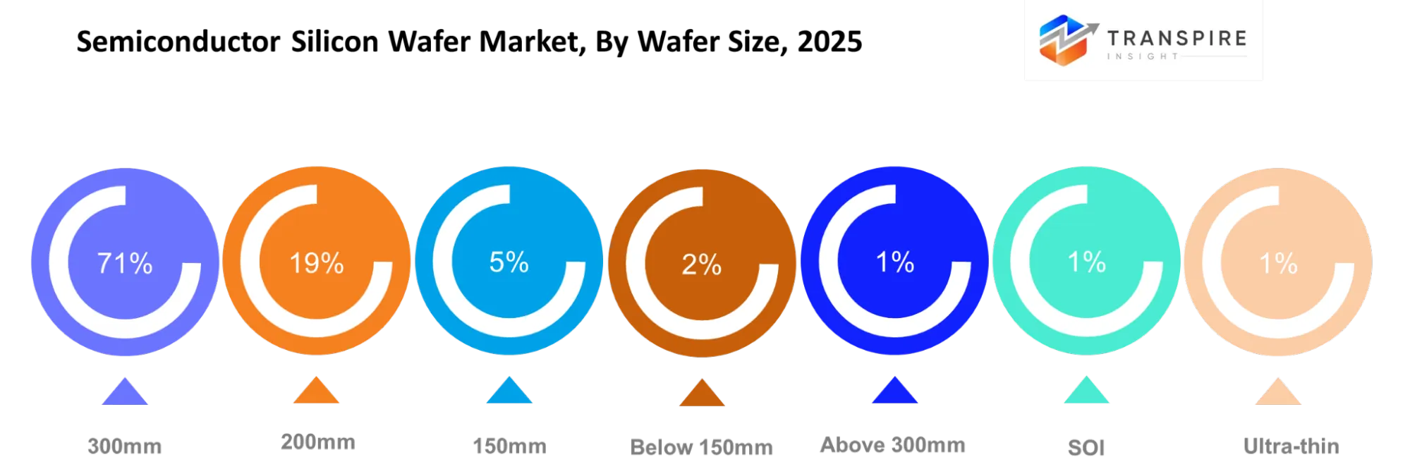
300mm wafers dominate at 71%, reflecting superior die-per-wafer economics for advanced logic and memory production. 200mm wafers account for 19%, retaining importance in mature-node, analogue, power, and speciality devices. 150mm represents 5%, while below 150mm contributes 2%. Above 300mm stands at 1%, alongside SOI at 1%, while Ultra-thin and Others each hold 0.5%. Future demand increasingly favours larger substrates and application-specific formats as fabs balance productivity, device complexity, and manufacturing economics.
By Type:
Polished wafers form the core substrate category because their controlled surface quality supports mainstream semiconductor fabrication. Epitaxial wafers add engineered layers for power, logic, and specialised devices, while Silicon-on-Insulator substrates support RF, photonics, and advanced architectures. Annealed and diffusion wafers address specific electrical and thermal requirements. Reclaimed wafers help reduce substrate consumption during process development, while test wafers support equipment qualification and yield engineering. This mix increasingly reflects specialisation rather than reliance on standardised substrates alone across semiconductor manufacturing applications and process platforms.
By Application:
Logic and Memory remain closely linked to advanced computing, AI accelerators, and high-performance data-centre infrastructure. Analogue and Power applications maintain broad exposure to automotive electrification, industrial controls, and energy systems, while MEMS supports sensing and automation. RF wafers serve wireless connectivity and communications equipment, and Image Sensors support smartphones, automotive vision, and machine vision. Future application growth increasingly depends on heterogeneous computing, vehicle electronics, edge intelligence, and specialised semiconductor architectures requiring differentiated wafer characteristics, electrical performance, and process compatibility across diverse end-use environments.
By Technology Node:
Above 65nm continues to support mature industrial, automotive, power, and control devices where proven processes remain economically attractive. The 45-65nm, 28-45nm, and 16-28nm ranges serve established high-volume applications requiring balanced performance and manufacturing efficiency. Meanwhile, 7-16nm, 5-7nm, and Below 5nm nodes support leading-edge processors, accelerators, and advanced computing. As geometries shrink, wafer requirements become increasingly stringent for flatness, contamination control, defect density, and uniformity, raising the importance of precision substrate manufacturing, metrology, and rigorous customer qualification processes.
By End User:
Foundries and Memory Manufacturers anchor high-volume 300mm wafer consumption because outsourced chip production and memory scaling require substantial substrate throughput. IDMs maintain integrated demand across logic, power, analogue, and speciality devices, while Fabless Companies influence wafer specifications through foundry relationships. Research Institutes support experimental process development and advanced materials evaluation. OSATs and Equipment Manufacturers consume wafers for packaging, testing, process qualification, and tool development. Future procurement will increasingly emphasise reliable supply, qualification continuity, geographical resilience, and application-specific substrate performance across semiconductor manufacturing ecosystems.
By Manufacturing Process:
Czochralski remains central to bulk silicon crystal production because it supports scalable semiconductor-grade substrates. Float Zone processing serves specialized applications requiring very high purity and controlled electrical properties. Epitaxy adds precisely engineered layers, while polishing establishes surface flatness and defect control required for fabrication. Cleaning removes contaminants, Annealing modifies material properties, and Doping adjusts electrical characteristics. Together, these stages increasingly determine wafer yield, reliability, and device performance, making process integration, automation, inspection, and metrology critical competitive factors for manufacturers globally.
By Material Grade:
Prime Grade represents the principal production category because advanced fabs require extremely low defect levels and consistent electrical properties. Test Grade and Reclaimed wafers support equipment qualification, process development, and engineering activities at lower substrate costs. Epi-grade wafers enable controlled surface layers for specialised device structures, while High-resistivity and Low-resistivity grades address different electrical requirements. Ultra-high purity materials support demanding applications where contamination can affect yield. Future differentiation increasingly centres on purity, defect control, resistivity, surface quality, and application-specific specifications as semiconductor architectures become more demanding.
What key use cases are driving the Semiconductor Silicon Wafer Market?
The original primary use is in high-volume chip manufacturing; 300mm accounts for 71% of volume. Large substrates improve die-per-wafer economics for advanced logic and memory. This directly supports production of the AI accelerators, data-centre processing chips and high-bandwidth memory.
Other uses include power-management ICs, automotive electronics, analogue, RF, MEMS and image sensors. The 200mm market remains important as many products use mature nodes and specific process types instead of advanced geometries.
Emerging applications are developing in photonics, AI infrastructure power devices and speciality substrates including SOI, epitaxial and high-resistivity wafers. These applications require tightly controlled electrical properties and defect performance, providing additional value over standard volume wafers.
|
Report Metrics |
Details |
|
Market size value in 2025 |
USD 14.49 Billion |
|
Market size value in 2026 |
USD 15.75 Billion |
|
Revenue forecast in 2033 |
USD 28.24 Billion |
|
Growth rate |
CAGR of 8.70% from 2026 to 2033 |
|
Base year |
2025 |
|
Historical data |
2021 - 2024 |
|
Forecast period |
2026 - 2033 |
|
Report coverage |
Revenue forecast, competitive landscape, growth factors, and trends |
|
Regional scope |
United States; Canada; Mexico; United Kingdom; Germany; France; Italy; Spain; Denmark; Sweden; Norway; China; Japan; India; Australia; South Korea; Thailand; Brazil; Argentina; South Africa; Saudi Arabia; United Arab Emirates |
|
Key companies profiled |
Shin-Etsu Chemical, SUMCO, GlobalWafers, Siltronic, SK Siltron, Soitec, Wafer Works, Okmetic, Simgui, Siltronix Silicon Technologies, Virginia Semiconductor, Episil, Ferrotec, GRINM Semiconductor Materials, Mimasu Semiconductor Industry. |
|
Customization scope |
Free report customization (country, regional & segment scope). Available customised purchase options to meet your exact research needs. |
|
Report Segmentation |
By Wafer Size (150mm, 200mm, 300mm, Below 150mm, Above 300mm, Ultra-thin Wafers, SOI Wafers, Others); By Type (Polished Wafers, Epitaxial Wafers, Silicon-on-Insulator, Annealed Wafers, Diffusion Wafers, Reclaimed Wafers, Test Wafers, Others); By Application (Logic, Memory, Analog, Power, MEMS, RF, Image Sensors, Others); By Technology Node (Above 65nm, 45-65nm, 28-45nm, 16-28nm, 7-16nm, 5-7nm, Below 5nm, Others); By End User (Foundries, IDMs, Memory Manufacturers, Fabless Companies, Research Institutes, OSATs, Equipment Manufacturers, Others); By Manufacturing Process (Czochralski, Float Zone, Epitaxy, Polishing, Cleaning, Annealing, Doping, Others); By Material Grade (Prime Grade, Test Grade, Reclaimed, Epi-grade, High-resistivity, Low-resistivity, Ultra-high purity, Others). |
Which Regions are Driving the Semiconductor Silicon Wafer Market Growth?
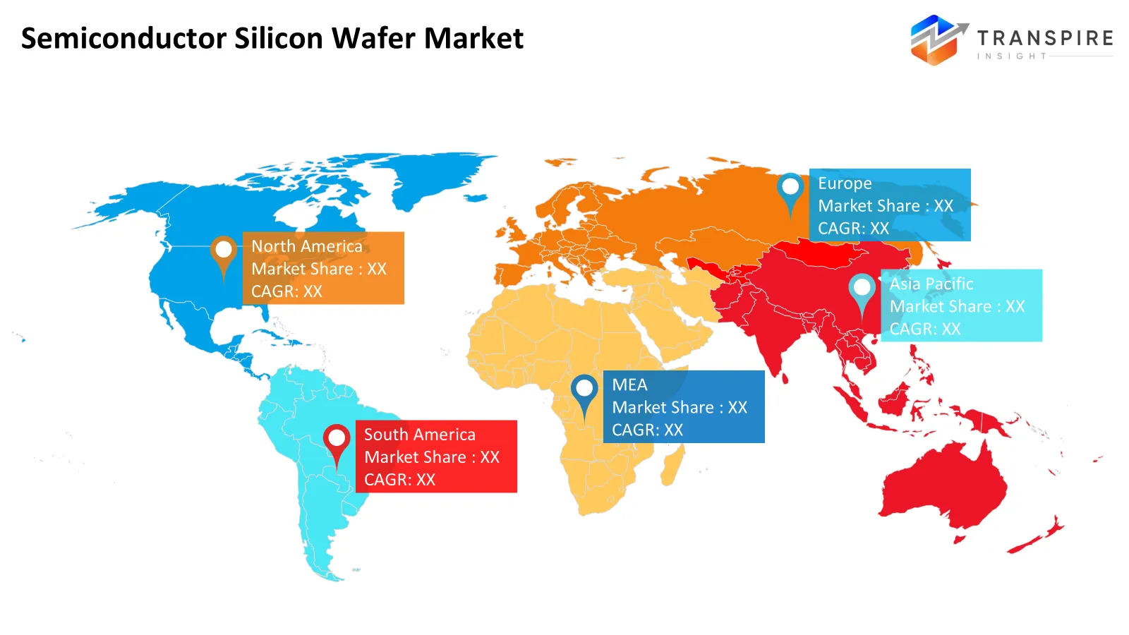
The Asia Pacific space comprised 78% of the market for semiconductor silicon wafers, the largest regional manufacturing base in the world. Foundry, memory, wafer, equipment, and materials ecosystems are all highly localized in Taiwan, South Korea, Japan, and China, with existing 300mm and 200mm fabs allowing suppliers to serve high-volume logic and memory programs with lower qualification times. Continuous growth in semiconductor capacity and artificial intelligence investment further enhances regional wafer demand and supplier concentration.
In September 2026, SEMI and Silicon Catalyst finalized a strategic partnership via a Memorandum of Understanding at SEMICON Taiwan 2026 to accelerate semiconductor innovation.
Europe makes up for 9% which is dramatically lower than Asia Pacific; but its position is reiterated by manufacturing of specialty wafers for MEMS, RF, power, sensors, and automotive applications. In contrast to the application scale-driven ecosystem of Asia Pacific, European suppliers focus on matching customized substrates and regional supply security with advanced specialty technology solutions. Okmetic's new plant in Finland has been in volume production since 2026, strengthening the regional availability of 150-200mm wafers in Europe.
In June 2026, Soitec partnered with ZenSemi to scale 300mm BCD-on-SOI production for next-generation power electronics. The partnership strengthens Europe’s specialty-substrate capabilities for energy-efficient power devices.
https://www.wsj.com/tech/soitec-shares-climb-on-partnership-with-chinas-zensemi-74a4ba0f
North America represents 10% of the market and is expected to grow at a CAGR of 6.4%, based on the semiconductor manufacturing's on-shoring and local supply chain investments. Wafers is also considering a second expansion step at the Texas 300mm plant following a USD 3.5 billion investment into the site. US incentives for local semiconductor manufacturing and semiconductor companies' investments to build or expand production result in additional demand for upstream wafer capacity and create opportunities for additional 300mm production, long-term supply commitments and improved sourcing resilience.
In July 2026, GlobalWafers secured a 10-year supply agreement alongside $500 million in strategic financing from Micron Technology. The partnership directly strengthens regional sourcing resilience by granting Micron guaranteed domestic access to critical wafer inputs for its U.S.-based DRAM and NAND memory chip production.
Who are the Key Players in the Semiconductor Silicon Wafer Market, and how do they compete?
Competitiveness is increasingly focused on scale, 300mm production, speciality substrates, quality uniformity, and geographic supply security. Shin-Etsu Chemical and SUMCO prioritise high-volume precision production and advanced 300mm capacity. GlobalWafers combines manufacturing capacity expansion with SOI, GaN and other high-end value-added products.
Siltronic applies advanced 300mm technology and geographic diversification, while SK Siltron utilises 200mm/300mm silicon production combined with speciality materials; Doosan agreed in 2026 to purchase 70.6% of SK Siltron. Soitec's focus on engineered substrates (namely SOI) for RF, auto and high-end computing provides differentiation; Wafer Works' areas of speciality include proven silicon wafer manufacturing, while Okmetic specialises in 150-200mm speciality wafers targeting MEMS, sensors, RF and power applications; its new Finnish facility entered volume manufacturing in 2026. Others competing on a regional basis in speciality substrates, customised specifications and application focus include Simgui, Siltronix Silicon Technologies, Virginia Semiconductor, Episil, Ferrotec, GRINM Semiconductor Materials and Mimasu Semiconductor Industry. Overall, it appears that differentiation strategies are shifting increasingly away from wafer volume to qualification, speciality applications, processing and customised specifications, and geographic supply security.
Key Players are:
- Shin-Etsu Chemical
- SUMCO
- GlobalWafers
- Siltronic
- SK Siltron
- Soitec
- Wafer Works
- Okmetic
- Simgui
- Siltronix Silicon Technologies
- Virginia Semiconductor
- Episil
- Ferrotec
- GRINM Semiconductor Materials
- Mimasu Semiconductor Industry
Recent Development News
- In July 2026, Doosan signed an agreement to acquire a 70.6% stake in SK Siltron for KRW 2.3 trillion. The transaction expands Doosan’s presence in semiconductor materials and supports the growth of SK Siltron’s 200mm and 300mm silicon wafer business. https://evertiq.com/design/2026-08-26-doosan-acquires-706-stake-in-sk-siltron
- In April 2026, SUMCO delayed construction of two planned silicon wafer fabs and redirected investment toward upgrading existing facilities. The move focuses capital on advanced wafer manufacturing capabilities and next-generation products while allowing the company to respond more flexibly to changing semiconductor demand. https://www.trendforce.com/news/2026/04/06/news-sumco-delays-construction-of-two-silicon-wafer-fabs-amid-market-shift/
- In September 2026, Wacker Chemie completed an institutional block placement to sell a portion of its remaining shares in hyperpure silicon wafer supplier Siltronic for gross proceeds of €171 million. This transaction optimises Wacker's corporate capital allocation for core growth industries, while expanding Siltronic’s institutional free-float ownership to better support artificial intelligence infrastructure demand. https://www.wacker.com/cms/en-us/press-and-media/press/press-releases/2026/press-releases-detail-2026-318144.html
What Strategic Insights Define the Future of the Semiconductor Silicon Wafer Market?
The market is heading toward a more segmented supply structure in which 300mm capacity supports AI, memory, and advanced logic while 150-200mm and engineered substrates remain essential for power, MEMS, RF, and industrial devices. The hidden risk is capacity timing: simultaneous government-backed fab expansion can create localized overcapacity before customer qualifications and utilization catch up, pressuring wafer economics. Okmetic has already highlighted uneven recovery and capacity additions as sources of market uncertainty. The emerging opportunity is localized wafer manufacturing, particularly where semiconductor incentives are linking domestic fabs with upstream material supply. GlobalWafers' Texas expansion demonstrates this direction. Strategically, suppliers should prioritize long-term customer qualification, specialty-wafer differentiation, and flexible regional capacity rather than pursuing volume expansion alone. This approach can protect utilization while capturing AI-driven demand and reducing exposure to geopolitical and logistics disruptions.
Key Segmentations are:
By Wafer Size
- 150mm
- 200mm
- 300mm
- Below 150mm
- Above 300mm
- Ultra-thin Wafers
- SOI Wafers
- Others
By Type
- Polished Wafers
- Epitaxial Wafers
- Silicon-on-Insulator
- Annealed Wafers
- Diffusion Wafers
- Reclaimed Wafers
- Test Wafers
- Others
By Application
- Logic
- Memory
- Analog
- Power
- MEMS
- RF
- Image Sensors
- Others
By Technology Node
- Above 65nm
- 45-65nm
- 28-45nm
- 16-28nm
- 7-16nm
- 5-7nm
- Below 5nm
- Others
By End User
- Foundries
- IDMs
- Memory Manufacturers
- Fabless Companies
- Research Institutes
- OSATs
- Equipment Manufacturers
- Others
By Manufacturing Process
- Czochralski
- Float Zone
- Epitaxy
- Polishing
- Cleaning
- Annealing
- Doping
- Others
By Material Grade
- Prime Grade
- Test Grade
- Reclaimed
- Epi-grade
- High-resistivity
- Low-resistivity
- Ultra-high purity
- Others
By Regional Analysis
North America
- US
- Canada
- Mexico
Europe
- Germany
- UK
- France
- Italy
- Spain
- Russia
- Rest of Europe
Asia Pacific
- China
- Japan
- India
- South Korea
- Australia
- Rest of Asia Pacific
South America
- Brazil
- Argentina
- Rest of South America
Middle East & Africa
- UAE
- Saudi Arabia
- Qatar
- South Africa
- Rest of the Middle East & Africa
Frequently Asked Questions
Find quick answers to common questions.
The semiconductor silicon wafer market size was valued at USD 14.49 billion in 2025 and is poised to reach USD 28.24 billion by 2033, expanding at an 8.70% CAGR.
Key segments for the Keyword are By Wafer Size (150mm, 200mm, 300mm, Below 150mm, Above 300mm, Ultra-thin Wafers, SOI Wafers, Others); By Type (Polished Wafers, Epitaxial Wafers, Silicon-on-Insulator, Annealed Wafers, Diffusion Wafers, Reclaimed Wafers, Test Wafers, Others); By Application (Logic, Memory, Analog, Power, MEMS, RF, Image Sensors, Others); By Technology Node (Above 65nm, 45-65nm, 28-45nm, 16-28nm, 7-16nm, 5-7nm, Below 5nm, Others); By End User (Foundries, IDMs, Memory Manufacturers, Fabless Companies, Research Institutes, OSATs, Equipment Manufacturers, Others); By Manufacturing Process (Czochralski, Float Zone, Epitaxy, Polishing, Cleaning, Annealing, Doping, Others); By Material Grade (Prime Grade, Test Grade, Reclaimed, Epi-grade, High-resistivity, Low-resistivity, Ultra-high purity, Others).
Growth is primarily driven by AI and data-center semiconductor expansion, HBM and advanced memory production, 300mm wafer adoption, advanced-node migration, semiconductor fab investments, and regional supply-chain localization.
Major manufacturers lead the semiconductor silicon wafer market, including Shin-Etsu Chemical, SUMCO, GlobalWafers, Siltronic, SK Siltron, Soitec, Wafer Works, Okmetic, Simgui, Siltronix Silicon Technologies, Virginia Semiconductor, Episil, Ferrotec, GRINM Semiconductor Materials, and Mimasu Semiconductor Industry.
Asia Pacific accounts for 78% of the market, driven by concentrated wafer manufacturing, foundries, memory fabs, semiconductor equipment suppliers, established 200mm/300mm infrastructure, and strong regional semiconductor investment.
Opportunities include domestic 300mm wafer capacity, AI-driven advanced wafers, SOI and specialty substrates, reclaimed wafers, and localized supply networks across India, Southeast Asia, and North America.
- Shin-Etsu Chemical
- SUMCO
- GlobalWafers
- Siltronic
- SK Siltron
- Soitec
- Wafer Works
- Okmetic
- Simgui
- Siltronix Silicon Technologies
- Virginia Semiconductor
- Episil
- Ferrotec
- GRINM Semiconductor Materials
- Mimasu Semiconductor Industr
About the Authors

Avinash Kumar
I’m Avinash Kumar, a Senior Research Analyst at Transpire Insight, with expertise in the Electronics and Semiconductor and Energy & Power industry. My work focuses on analyzing emerging technologies, market trends, industry developments, and innovation across these sectors. I specialize in transforming complex technical and market insights into clear, research-backed content that helps professionals, businesses, and decision-makers stay informed. Through continuous industry research and data-driven analysis, I strive to deliver accurate, reliable, and practical perspectives on the latest advancements shaping the semiconductor and energy landscape.

Chakradhar Khansole
Chakradhar serves as the Research Director at Transpire Insight, bringing over 8 years of experience in technology, innovation, and strategic market intelligence. He specializes in transforming complex market data into actionable business insights that enable organizations to make informed, growth-oriented decisions. Recognized for his strategic vision and analytical expertise, Chakradhar leads high-impact research initiatives, delivering comprehensive market assessments, competitive intelligence, and forward-looking industry analysis.
Recently Published Reports
-
Apr 2026
Fiber Optic Faceplates Market
Fiber Optic Faceplates Market Size, Share & Analysis Report By Type (< 300 mm2, 300-350 mm2, and > 350 mm2, By Application (Night Vision, Holographic Imaging, Medical, and Others), and Geography (North America, Europe, Asia-Pacific, Middle East and Africa, South and Central America), 2021 - 2031
-
Apr 2026
High Temperature Superconductors Market
High Temperature Superconductors Market Size, Share & Analysis Report By Type (1G HTS, and 2G HTS), By Application (Power Cable, Fault Current Limiter, and Transformer), and Geography (North America, Europe, Asia-Pacific, Middle East and Africa, South and Central America), 2021 - 2031
-
Apr 2026
Industrial Plugs and Socket Market
Industrial Plugs and Socket Market Size, Share & Analysis Report By Type (Industrial Plugs, Industrial Sockets), By Current (Up to 32 A, 32 to 125 A, Above 125 A), By Protection (Dustproof and Splash Proof, Waterproof, Explosion Proof), By End User (Heavy Industries, Oil and Gas, Chemicals and Pharmaceuticals, Power Generation, Others), and Geography (North America, Europe, Asia-Pacific, Middle East and Africa, South and Central America), 2021 - 2031
-
Apr 2026
InGaAs Avalanche Photodiodes Market
InGaAs Avalanche Photodiodes Market Size, Share & Analysis Report By Type (1100 - 1700 nm, and 1000 - 1600 nm), By Application (Missile Warning System, Muzzle Flash Detection, Wafer Defect Inspection, Laser Rangefinders, and Others), and Geography (North America, Europe, Asia-Pacific, Middle East and Africa, South and Central America), 2021 - 2031