

Japan GAN Epitaxial Wafers Market Summary:
According to Transpire Insights, a detailed research report on the market reflects that the GaN-based epitaxial wafers segment dominates the Japan LED Epitaxial Wafer Market, accounting for approximately 69.60% of the total material-system share in 2025. Sumitomo Chemical leads Japan’s GaN epitaxial wafer industry with advanced MOVPE-grown GaN epiwafer capabilities for high-electron-mobility transistors (HEMTs) and high-voltage power devices, making it a key contributor to Japan market development, innovation, advanced GaN epitaxial wafer production, expanding manufacturing capabilities, and growth dynamics.
Market Snapshot
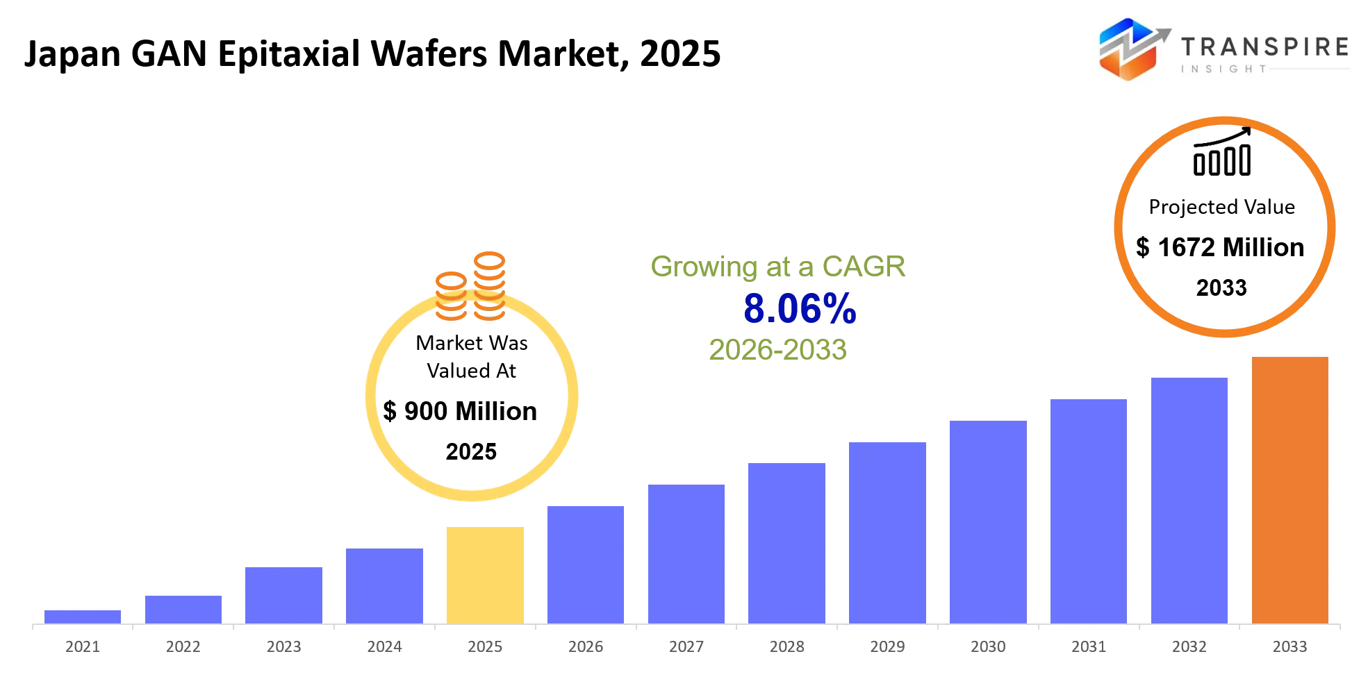
- Market Value (2025): USD 900 Million.
- Expected Market Value (2026): USD 972 Million.
- Estimated Market Value (2033): USD 1672 Million.
- Forecast CAGR (2026–2033): 8.06%
Introduction
The GaN epilayer wafers contain a base substrate wafer such as silicon, silicon carbide, or sapphire on which a very thin and exact layer of GaN is formed using methods of epitaxy. Such epitaxy techniques include Metal-Organic Chemical Vapor Deposition (MOCVD) and Hydride Vapor-Phase Epitaxy (HVPE). With GaN’s large band gap and electron mobility, these wafers allow electronics to be operated at higher switching rates, voltages, and with improved thermal efficiency compared to silicon wafers. GaN (Gallium Nitride) is a wide-bandgap semiconductor. In contrast to the conventional silicon, GaN can endure much higher voltages, temperatures, and switching rates before failing. It is simply a super-strong variant of silicon. Advanced semiconductor technologies offer several performance advantages that support their growing adoption across high-power and high-frequency applications. High breakdown voltage enables reliable operation under demanding electrical conditions, improving device durability and system safety. Superior electron mobility facilitates rapid charge transport, supporting ultra-fast switching and high-frequency power conversion. Enhanced thermal efficiency enables stable performance under elevated temperatures and high power densities, reducing thermal management challenges. Low on-resistance (RDS(on)) minimizes conduction losses and improves overall power efficiency. Together, these characteristics enhance switching performance, energy efficiency, reliability, and power density, making advanced semiconductor devices suitable for electric vehicles, renewable energy, data centers, and industrial power systems.
Key Market Highlights: -
- By substrate, the SiC segment dominated the market and holds nearly 45% share in 2025 and is projected to grow at a substantial CAGR during the forecast period.
- By application, the Automotive segment dominated the market and holds nearly 34% share in 2025 and is projected to grow at a substantial CAGR during the forecast period.
- By end user, the Foundries segment dominated the market and holds nearly 50% share in 2025 and is projected to grow at a substantial CAGR during the forecast period.
- The Japanese government is bolstering the country’s semiconductor supply chain through significant investments in advanced semiconductor technology. The METI framework has provided more than ¥10 trillion worth of public support till fiscal year 2030, which includes programs for the next-generation of power semiconductors such as GaN and SiC. This favorable policy climate ensures investment, technological advancement in wafer technology, increased production capacity, and strengthens the supply chain.
How is Technology Driving Growth in the Japan GAN Epitaxial Wafers Market?
The Japan GaN epitaxial wafers market will be progressing through improvements in the MOCVD and HVPE process, increasing the quality of crystals and decreasing the defect density. The adoption of 6-inch and 8-inch wafer sizes will increase efficiency, increase yields, and contribute to cost savings. The rising need for electric vehicles due to their growing electrification requires the use of highly-efficient GaN-based power components in advanced EV power system. On the other hand, the development of 5G and upcoming 6G infrastructure is enabling the use of GaN in RF technologies for high-power and high-frequency operations. Simultaneously, R&D, manufacturing activities, and national semiconductor initiatives in Japan will improve the Japanese advanced semiconductor industry.
Market Drivers
The Japan GaN Epitaxial Wafers Market is being fueled by growth in the market for electric vehicles and charging stations, increasing demand for high-voltage GaN power devices, and rapid deployment of AI and data centers. The development of 5G and RF infrastructure will further drive demand for high-frequency GaN semiconductors and epitaxial wafers. Moreover, the use of Mini LEDs and Micro LEDs for display applications is helping in the expansion of GaN semiconductor products. The investment of Japanese semiconductor makers in strategic activities domestically, such as ROHM Semiconductor, is building their epitaxy capacity. The Japanese GaN epitaxial wafers industry enjoys the advantage of having precise manufacturing processes through sophisticated robots and automation. Japan has well-established infrastructure in the semiconductor industry and investment in integrated fabrication systems and clean handling of high purity material. Japan has technological specialization in the field of GaN materials, GaN epitaxy, and high performance power devices that have to be made smaller. Moreover, the focus of Japan on sustainability and energy efficiency is boosting the demand for low loss semiconductors and power conversion technology.
Restrain
The Japan GaN Epitaxial Wafers Market is marked by high manufacturing costs, technical difficulties, expensive investments, geopolitical rivalry, and long qualification procedures. Complicated MOCVD and HVPE manufacturing processes raise production costs, whereas the production of high-quality wafers with large diameters and low defects is difficult to achieve. Expensive cleanrooms constitute a barrier to entry, fierce competition exerts pressure on prices, and tough automotive and military qualifications limit supplier implementation.
|
Driver |
Relative Impact on Growth (%) |
Geographic Relevance |
Impact Timeline |
Demand Strength |
Growth Mechanism |
Key Beneficiaries |
Major Constraint |
|
AI Data Centers & High-Efficiency Power Conversion |
28% |
Japan; Asia Pacific; North America |
Short-term |
High |
AI servers require higher-efficiency GaN power conversion |
Epiwafer makers; power-device fabs; data-center OEMs |
Qualification cycles slow rapid GaN adoption |
|
EV & Automotive Electrification |
23% |
Japan; Asia Pacific; Europe |
Medium-term |
High |
EV power conversion increases demand for high-voltage GaN |
Epi suppliers; automotive semiconductor makers; Tier-1s |
SiC remains strong for high-power applications |
|
Government Semiconductor & Energy-Efficiency Support |
19% |
Japan |
Short-term |
High |
Public funding accelerates GaN R&D and production capacity |
Domestic epi suppliers; device manufacturers; equipment vendors |
Subsidy dependence can distort investment timing |
|
Large-Diameter Wafer Scaling |
17% |
Japan; Asia Pacific |
Medium-term |
High |
6/8-inch scaling improves throughput and lowers unit costs |
Epiwafer producers; fabs; equipment suppliers |
Defect control and wafer bow remain challenging |
|
RF, 5G/6G & Defense Electronics |
13% |
Japan; North America; Asia Pacific |
Long-term |
Medium |
High-frequency GaN increases premium RF epi demand |
RF epi suppliers; telecom; aerospace/defense |
High qualification costs restrict supplier switching |
Analysis of Prices and Consumer Behaviour
The market for GaN epitaxial wafers is dominated by GaN-based epitaxial wafers (69.60% of the Japan LED epitaxial wafer market in 2025; primarily due to the demand from automotive lighting, displays, UV sterilization and industrial applications). The Japan GaN HEMT epitaxial wafer market was valued at roughly USD 32.46 million in 2025 and is projected to reach USD 57.28 million by 2032, registering an 8.2% CAGR. Around 44.20% of Japan’s LED epitaxial wafer market consisted of 150 mm wafers in 2025. The sales volume is driven by demand for advanced semiconductor applications and larger wafer formats. The Japan LED epitaxial wafer market was valued at USD 180.7 million in 2025 and is projected to reach USD 296.4 million by 2031, growing at an 8.80% CAGR.
Who are the Key Players in the Japan GAN Epitaxial Wafers Market and how do they compete?
Competitive advantage on the international market of GaN epitaxial wafers relies on companies which specialize in advanced epitaxial growth technologies, high-quality wafer manufacturing, semiconductor material innovation, and development of high-performance GaN solutions for applications in power electronics, RF devices, 5G communications, automotive electronics and consumer electronics. Competing not only on price, but through advanced capabilities in wafer quality, epitaxial layer uniformity, defect reduction, substrate compatibility, manufacturing scalability and customized wafer specifications, such competitive approach results in continuous technological innovation and enables organizations to improve semiconductor performance, power efficiency, reliability and device miniaturization.
By developing high-quality GaN epitaxial wafers, advanced compound semiconductor materials, and specialized epitaxial growth technologies, Fujitsu, Sumitomo Electric Industries, and SCIOCS increase their competitive position on the Japan GaN epitaxial wafers market. Developing high-performance GaN-on-Si, GaN-on-SiC and other epitaxial wafer solutions for power and RF semiconductor applications distinguishes companies from their competitors. Sumitomo Electric Industries increases its competitive position by providing advanced compound semiconductor materials and GaN-based solutions, while SCIOCS strengthens its position through specialized GaN epitaxial wafer technologies and high-quality semiconductor materials for demanding electronic applications.
Top Companies in the Japan GAN Epitaxial Wafers Market
- Sumitomo Electric
- Mitsubishi Chemical
- SCIOCS
- Furukawa Electric
- Panasonic
- ROHM
- Sony Semiconductor Solutions
- Fujitsu
- Toshiba
- Nagoya University Spin-off Companies
- IQE
- Coherent
- Wolfspeed
- Qorvo
- GlobalFoundries
|
Company |
Est. Revenue Share Range |
Key Offerings |
Strategic Positioning |
Geographic Strength |
Technology Focus |
|
Sumitomo Chemical Co., Ltd. |
22–30% (Estimated) |
AlGaN/GaN HEMT epi; GaN-on-SiC; GaN-on-GaN; high-voltage power epi |
Integrated Japanese leader across GaN epi platforms |
Asia Pacific; Japan; North America |
MOVPE, GaN-on-SiC, GaN-on-GaN, high-voltage epitaxy |
|
NTT Advanced Technology Corporation |
8–13% (Estimated) |
AlGaN/GaN HEMT; InAlN/GaN HEMT; p-GaN; custom epi structures |
Custom epi supplier for RF, power, R&D |
Japan; Asia Pacific; Global R&D |
AlGaN/GaN HEMT, InAlN/GaN, 6–8-inch Si epi |
|
Shin-Etsu Chemical Co., Ltd. |
8–12% (Estimated) |
QST substrates; GaN-grown QST; 6/8-inch platforms; 300-mm QST |
Large-diameter platform strategy via QST substrates |
Japan; Asia Pacific; North America |
QST, stress-managed thick GaN, 300-mm substrates |
|
Sanken Electric Co., Ltd. / POWDEC |
5–9% (Estimated) |
AlGaN/GaN HEMT epi; GaN/sapphire templates; AlN templates |
Vertical integration around proprietary GaN epitaxy |
Japan; Asia Pacific |
PSJGaN, GaN HEMT epitaxy, GaN crystal growth |
|
IQE plc |
5–9% (Estimated) |
GaN RF HEMT; 650V D/E-mode; vertical GaN-on-GaN; microLED epi |
Global scale with broad GaN epi portfolio |
Europe; North America; Asia Pacific |
MOCVD/MBE, GaN-on-SiC, GaN-on-Si, GaN-on-GaN |
|
Enkris Semiconductor Inc. |
4–7% (Estimated) |
GaN-on-Si power epi; RF epi; microLED epi; GaN templates |
Cost-efficient large-diameter GaN-on-Si specialist |
Asia Pacific; Japan; China |
200/300-mm GaN-on-Si, buffer engineering, HEMTs |
|
Sumitomo Electric Industries, Ltd. |
3–6% (Estimated) |
GaN/SiC RF epi structures; GaN HEMTs; advanced RF materials |
RF-focused vertical integration and domestic supply |
Japan; North America; Asia Pacific |
GaN-on-SiC, RF HEMTs, advanced heterostructures |
|
Soitec / Soitec Belgium |
2–5% (Estimated) |
RF-GaN epi; AlGaN/GaN; InAlN/GaN; SiC-based RF epi |
Engineered-substrate ecosystem and RF specialization |
Europe; Asia Pacific; North America |
Fe-free buffers, in-situ SiN, 150/200-mm RF-GaN |
|
SweGaN AB |
2–4% (Estimated) |
QuanFINE GaN-on-SiC; RF epi; power epi; customized structures |
Premium performance through buffer-free GaN-on-SiC |
Europe; Japan/Asia; North America |
QuanFINE, buffer-free epi, high-mobility GaN-on-SiC |
|
WaveLord Co., Ltd. |
1–3% (Estimated) |
RF GaN-on-SiC; 8-inch power GaN-on-Si; p-GaN HEMT epi |
Emerging Korean challenger targeting RF and power |
Asia Pacific; Japan; Korea |
p-GaN E-mode, 8-inch GaN-on-Si, GaN-on-SiC |
Japan GAN Epitaxial Wafers Market Segmentation
The Japan GAN Epitaxial Wafers Market share is divided into six categories: By substrate, wafer size, device, application, growth method and end user.
The SiC dominated the market, accounting for nearly 45% in 2025 and is expected to rise at a significant CAGR during the forecast period.
The Japan GAN Epitaxial Wafers Market is segmented by substrate into Silicon, Sapphire, SiC, GaN, Diamond, Glass, Other Substrates. Among these, the SiC segment dominated the market, accounting for nearly 45% in 2025 and expected to increase at a significant CAGR during the forecast period. SiC was leading the market during 2025 due to the presence of factors such as high breakdown voltage, better thermal conductivity, and low switching losses. The wide adoption of SiC power semiconductors in applications such as EVs, renewable energy systems,laser diode and industrial power electronics drives the growth of the market.
The Automotive dominated the market, accounting for nearly 34% in 2025, and is expected to rise at a significant CAGR during the forecast period.
The Japan GAN Epitaxial Wafers Market is segmented by application into, 5G Infrastructure, Power Electronics, Consumer Electronics, Automotive, Aerospace & Defense, Data Centers, Renewable Energy, Industrial. Among these, the Automotive segment dominated the market, accounting for nearly 34% in 2025 and expected to increase at a significant CAGR during the forecast period. Automotive was the dominant sector in 2025 due to growing vehicle electrification trends and increased application of sophisticated power semiconductors. Silicon carbide (SiC) devices exhibit high efficiency and voltage-handling ability and can be used in electric vehicles (EVs), including EV inverters and chargers. Increased EV production and growing demand for energy-efficient power systems drive automotive sector growth.
The Foundries dominated the market, accounting for nearly 50% in 2025 and is expected to rise at a significant CAGR during the forecast period.
The Japan GAN Epitaxial Wafers Market is segmented by end user into Semiconductor Manufacturers, Foundries, Device Manufacturers, Research Institutes, Telecom Companies, Automotive OEMs, Power Electronics Companies, LED Manufacturers. Among these, the Foundries segment dominated the market, accounting for nearly 50% in 2025 and expected to increase at a significant CAGR during the forecast period. Foundries held dominance in the market by occupying almost 50% in 2025 due to factors such as increased outsourcing of semiconductors, growing need for advanced manufacturing processes, and the use of specialized process technology. Foundries help in cost-effective and scalable manufacturing of chips while catering to automotive, consumer electronics, telecoms, and industries applications.
Future Market Trends for the Japan GAN Epitaxial Wafers Market: -
- Electrification of Automotive: Extensive use of GaN-based inverters and on-board charging systems to increase the range of electric vehicles and cut thermal losses.
- AI Servers/Data Centers: Use of highly efficient power systems to manage increasing energy demands arising from AI-powered computational facilities.
- Domestic Upstream Integration: Significant efforts by Japanese chemical and semiconductor companies to increase production capacity of bulk GaN substrates and epitaxies domestically.
- Smart Factory Automation: Use of AI-powered quality control and digital twins during the manufacturing of wafers to lower defect levels.
- Mini/micro-LED Growth: Increased adoption of MOCVD process in automotive adaptive lighting and display applications.
Recent Development
- In June 2026: The G10-GaN deposition system offered by AIXTRON was chosen by ROHM Semiconductor for its own production of GaN epitaxial wafers in the company’s Hamamatsu factory. The equipment enables mass manufacturing of 8-inch GaN epitaxial wafers for 650 V and 100 V power devices, which will benefit the Japanese GaN epitaxial wafers market.
- In July 2026: The Mitsubishi Chemical Group and Japan Steel Works plan to raise the capacity for manufacturing GaN substrates by 50 percent in 2027 relative to 2026 as a reaction to the increasing demand for future-generation power semiconductors for EVs, inverters, and power systems for data centers. This move will help boost Japan's GaN substrate value chain.
- In May 2026: Expansion of GaN production facilities by GlobalWafers to cater to growing demand for efficient power solutions in AI servers. This expansion plan reflects the growing need for power semiconductors based on GaN technology and provides an opportunity to the Asia-Pacific GaN supply chain. This expansion plan will further provide opportunities to the GaN epitaxial wafers market in Japan.
Market Segment
This study forecasts revenue at Japan, regional and country levels from 2020 to 2033. Transpire Insights has segmented the Japan GAN Epitaxial Wafers Market based on the below-mentioned segments:
Japan GAN Epitaxial Wafers Market, By Substrate
- Silicon
- Sapphire
- SiC
- GaN
- Diamond
- Glass
- Other Substrates
Japan GAN Epitaxial Wafers Market, By Wafer Size
- 2-Inch
- 4-Inch
- 6-Inch
- 8-Inch
- 12-Inch
- Small Diameter
- Large Diameter
- Custom Size
Japan GAN Epitaxial Wafers Market, By Device
- RF Devices
- Power Devices
- LEDs
- Laser Diodes
- 5G Devices
- HEMTs
- Micro-LEDs
- Optoelectronics
Japan GAN Epitaxial Wafers Market, By Application
- 5G Infrastructure
- Power Electronics
- Consumer Electronics
- Automotive
- Aerospace & Defense
- Data Centers
- Renewable Energy
- Industrial
Japan GAN Epitaxial Wafers Market, By Growth Method
- MOCVD
- MBE
- HVPE
- PAMBE
- Ammonothermal
- Epitaxial Regrowth
- CVD
- Other Methods
Japan GAN Epitaxial Wafers Market, By End User
- Semiconductor Manufacturers
- Foundries
- Device Manufacturers
- Research Institutes
- Telecom Companies
- Automotive OEMs
- Power Electronics Companies
- LED Manufacturers
Frequently Asked Questions
Find quick answers to common questions.
The market is projected to reach USD 1,672 million by 2033, expanding at an 8.06% CAGR from 2026–2033.
SiC substrates dominated in 2025, accounting for nearly 45%, supported by high breakdown voltage, thermal conductivity, and low switching losses.
Automotive accounted for nearly 34% in 2025, driven by vehicle electrification and increasing demand for advanced power semiconductor technologies.
AI data centers require high-efficiency power conversion, increasing demand for GaN-based power semiconductors and epitaxial wafers in Japan.
Key trends include automotive electrification, AI data centers, domestic integration, smart-factory automation, and Mini-LED/Micro-LED adoption through 2033.
- Sumitomo Electric
- Mitsubishi Chemical
- SCIOCS
- Furukawa Electric
- Panasonic
- ROHM
- Sony Semiconductor Solutions
- Fujitsu
- Toshiba
- Nagoya University Spin-off Companies
- IQE
- Coherent
- Wolfspeed
- Qorvo
- GlobalFoundries
About the Authors

Avinash Kumar
I’m Avinash Kumar, a Senior Research Analyst at Transpire Insight, with expertise in the Electronics and Semiconductor and Energy & Power industry. My work focuses on analyzing emerging technologies, market trends, industry developments, and innovation across these sectors. I specialize in transforming complex technical and market insights into clear, research-backed content that helps professionals, businesses, and decision-makers stay informed. Through continuous industry research and data-driven analysis, I strive to deliver accurate, reliable, and practical perspectives on the latest advancements shaping the semiconductor and energy landscape.

Chakradhar Khansole
Chakradhar serves as the Research Director at Transpire Insight, bringing over 8 years of experience in technology, innovation, and strategic market intelligence. He specializes in transforming complex market data into actionable business insights that enable organizations to make informed, growth-oriented decisions. Recognized for his strategic vision and analytical expertise, Chakradhar leads high-impact research initiatives, delivering comprehensive market assessments, competitive intelligence, and forward-looking industry analysis.
Recently Published Reports
-
Apr 2026
Fiber Optic Faceplates Market
Fiber Optic Faceplates Market Size, Share & Analysis Report By Type (< 300 mm2, 300-350 mm2, and > 350 mm2, By Application (Night Vision, Holographic Imaging, Medical, and Others), and Geography (North America, Europe, Asia-Pacific, Middle East and Africa, South and Central America), 2021 - 2031
-
Apr 2026
High Temperature Superconductors Market
High Temperature Superconductors Market Size, Share & Analysis Report By Type (1G HTS, and 2G HTS), By Application (Power Cable, Fault Current Limiter, and Transformer), and Geography (North America, Europe, Asia-Pacific, Middle East and Africa, South and Central America), 2021 - 2031
-
Apr 2026
Industrial Plugs and Socket Market
Industrial Plugs and Socket Market Size, Share & Analysis Report By Type (Industrial Plugs, Industrial Sockets), By Current (Up to 32 A, 32 to 125 A, Above 125 A), By Protection (Dustproof and Splash Proof, Waterproof, Explosion Proof), By End User (Heavy Industries, Oil and Gas, Chemicals and Pharmaceuticals, Power Generation, Others), and Geography (North America, Europe, Asia-Pacific, Middle East and Africa, South and Central America), 2021 - 2031
-
Apr 2026
InGaAs Avalanche Photodiodes Market
InGaAs Avalanche Photodiodes Market Size, Share & Analysis Report By Type (1100 - 1700 nm, and 1000 - 1600 nm), By Application (Missile Warning System, Muzzle Flash Detection, Wafer Defect Inspection, Laser Rangefinders, and Others), and Geography (North America, Europe, Asia-Pacific, Middle East and Africa, South and Central America), 2021 - 2031