
Semiconductor Metrology And Inspection Equipment Market Summary:
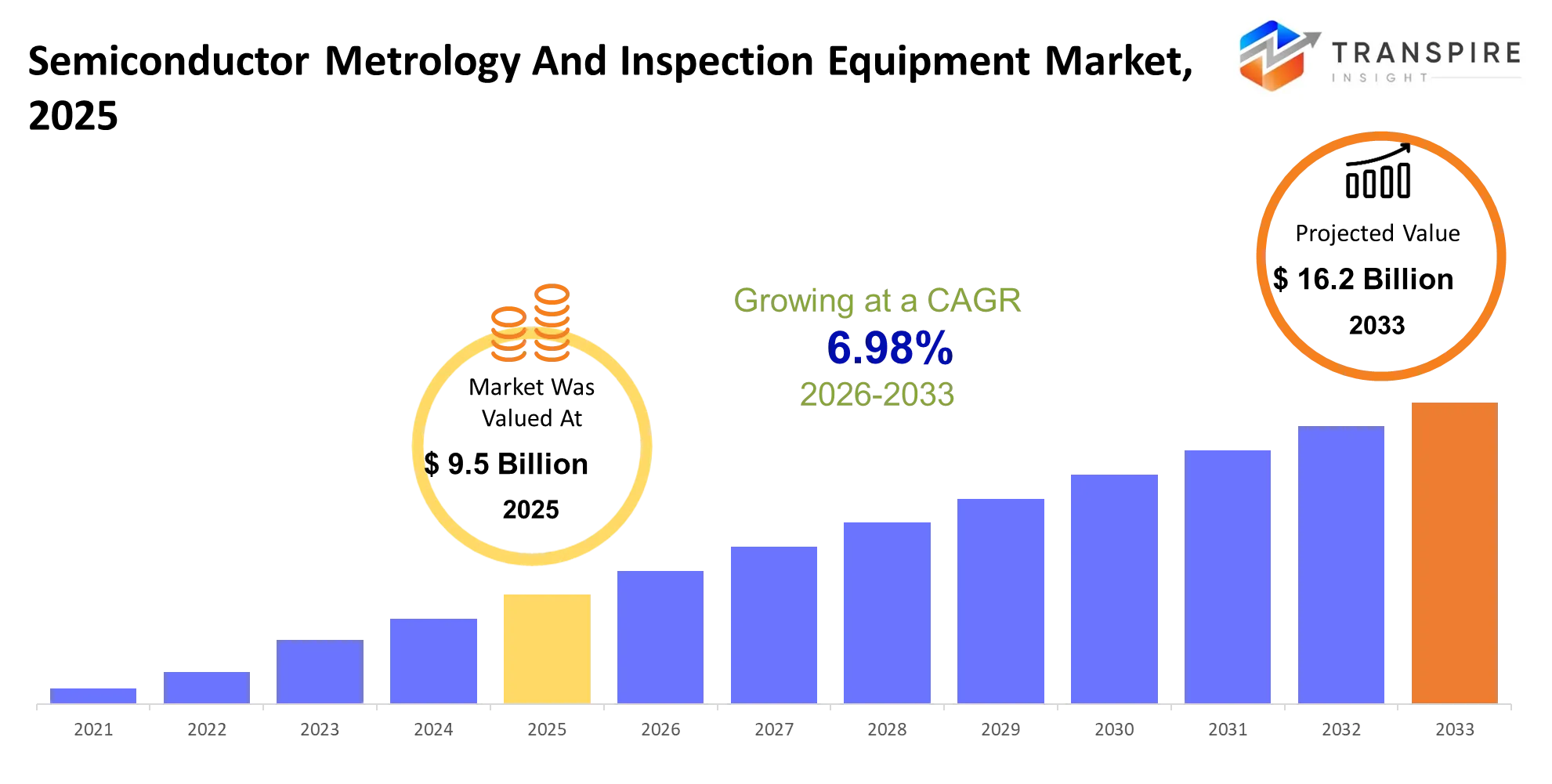
As per Transpire Insight, The Semiconductor Metrology and Inspection Equipment Market size is estimated at USD 9.5 billion in 2025 and is anticipated to reach USD 16.2 billion by 2033, growing at a CAGR of 6.98% from 2026 to 2033.
The semiconductor metrology and inspection equipment market provides chipmakers with precise metrology and defect-detection tools used to confirm wafer quality, mask correctness, thin-film thickness, and package integrity throughout the entire chip-manufacturing process. The market has been shifting from conventional optical inspection over the past three to five years to more AI-assisted hybrid metrology-which combines optical, e-beam, and computational metrology-for sub-5 nm manufacturing. Structural industry shifts have included moving to Advanced Packaging and High-NA EUV process control, which requires 50 times more measurement points per wafer than a 5 nm node. External drivers include government-led chip-building subsidy programs, such as the U.S. CHIPS Act and similar funding across Europe and Asia, which have sped up fab construction and equipment demand, and the never-ending quest to raise the bar on speed and precision will cause the number of measurement steps to grow, further lowering yield and driving equipment investment and fab spending.
Semiconductor Metrology And Inspection Equipment Market Size & Forecast:
- Market Size 2025: USD 9.5 billion
- Expected Market Value (2033): USD 16.2 billion
- Forecast CAGR (2026–2033): 6.98%
- Leading Region in 2025: Asia Pacific
- Fastest Growing Region: Europe
- Key Company Profiles: KLA Corporation, Applied Materials, ASML, Hitachi High-Tech, Lam Research, Onto Innovation, Nova Ltd., Lasertec, Thermo Fisher Scientific, Camtek, SCREEN Semiconductor Solutions, JEOL, Nikon, Carl Zeiss, Rigaku.
Key Semiconductor Metrology And Inspection Equipment Market Insights:
Medical component manufacturing is moving from traditional contract manufacturing to precision-engineered, validated components to support increasingly complex medical devices. Now it's all about material knowledge, regulatory tracking, and scalability without compromising quality.
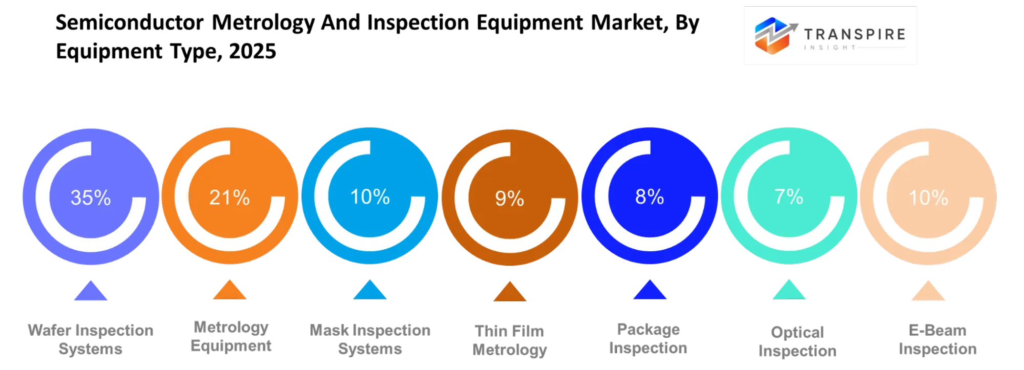
- Wafer inspection systems make up 35.00% of the market and are being enhanced with multi-beam imaging to cope with denser patterns for AI processors.
- KLA has a 53% market share of semiconductor inspection systems and, with its large installed base, is bringing analytics into every inspection and metrology process.
- Applied Materials owns approximately 15% and is developing digital-twin and predictive metrology tools to connect process equipment to virtual yield models.
- Around 11%, ASML is using its Hermes Microvision e-beam unit to match its inspection customers with EUV lithography customers.
- Hitachi High-Tech represents approximately 7.8% and is investing in high-resolution e-beam review for sub-7 nm defect characterisation.
- Onto Innovation is focusing on advanced packaging, and its Firefly platform measures substrate deformation and enables chiplet alignment.
- In April 2026, Camtek announced its acquisition of Visual Layer to provide visual AI solutions for defect classification in advanced packaging and high-density devices.
- With increasing mask-complexity demands from the major nodes, Lasertec is well positioned for EUV mask inspection.
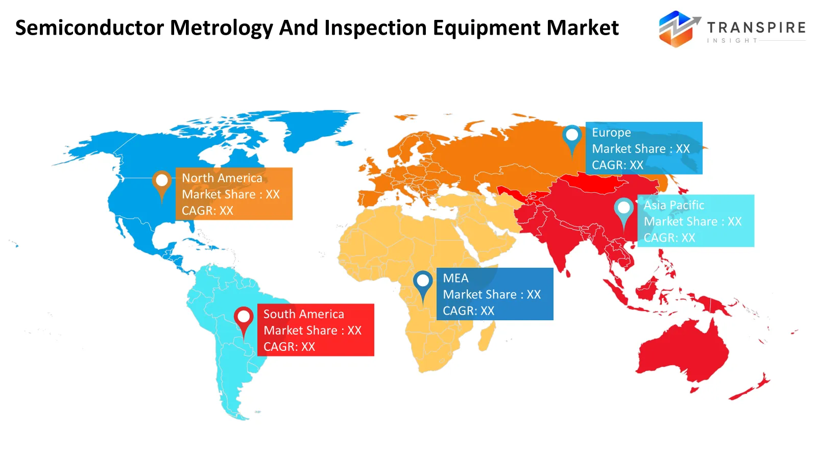
- Asia Pacific is the largest share of the market, accounting for 34.40% of the market due to the concentration of foundries, investment in advanced nodes, and growing packaging capacity.
What are the Key Drivers, Restraints, and Opportunities in the Semiconductor Metrology And Inspection Equipment Market?
Driver:
The strongest growth driver is the rapid transition toward advanced semiconductor nodes and heterogeneous packaging, which require significantly tighter process control than previous generations. This shift was triggered by AI accelerators, high-bandwidth memory, automotive electronics, and advanced computing chips that depend on extremely small geometries. As manufacturers add more inspection and metrology steps to prevent expensive wafer defects, equipment utilisation rises, improving production yields and expanding supplier revenues.
Restraint:
The biggest restraint is the exceptionally high ownership cost of advanced metrology platforms, particularly e-beam and High-NA EUV-compatible inspection systems. The challenge persists because these tools require sophisticated optics, vacuum systems, computational processing, and lengthy calibration procedures. Long development cycles, limited specialist suppliers, and complex integration into existing fabrication lines further slow purchasing decisions, especially for mid-sized manufacturers.
Opportunity:
A significant opportunity is emerging from advanced packaging, chiplet manufacturing, and regional semiconductor capacity expansion. Countries investing in domestic fabrication infrastructure are creating new demand for inspection systems across wafer processing, packaging, and final testing. For example, investments supporting 3D stacking, wafer-level packaging, and hybrid bonding require increasingly precise metrology throughout production. AI-enabled inspection software also opens opportunities by reducing analysis time and enabling predictive defect classification, allowing manufacturers to improve throughput while maintaining quality standards as production volumes continue expanding globally.
Driver Impact Analysis: Semiconductor Metrology and Inspection Equipment Market
|
Driver |
Relative Impact on Growth (%) |
Geographic Relevance |
Impact Timeline |
Demand Strength |
Growth Mechanism |
Key Beneficiaries |
Major Constraint |
|
AI chip demand and advanced-node manufacturing |
28% |
Taiwan, South Korea, United States |
Short-term (≤2 years) |
High |
Enables nanoscale defect detection and tighter process control |
KLA, Applied Materials, Nova, advanced-node foundries |
High equipment costs and complex process integration |
|
Rising HBM, 3D NAND and advanced packaging complexity |
23% |
South Korea, Taiwan, United States |
Short-term (≤2 years) |
High |
Increases demand for 3D inspection, overlay and dimensional metrology |
KLA, Onto Innovation, Applied Materials, memory manufacturers |
Difficult inspection of buried structures and stacked dies |
|
fab expansion and semiconductor localization incentives |
20% |
United States, China, Taiwan, Japan, India |
Medium-term (2–4 years) |
High |
New fabs require inspection tools, metrology systems, and service infrastructure |
Equipment OEMs, foundries, IDMs, local service providers |
Delayed fab construction and uncertain capital expenditure |
|
AI-enabled inspection and advanced process-control adoption |
16% |
United States, Japan, South Korea, Taiwan |
Medium-term (2–4 years) |
High |
Automates defect classification and improves yield-learning efficiency |
Inspection OEMs, AI software vendors, semiconductor fabs |
Data quality limitations and integration complexity |
|
Tighter yield, reliability, and export-compliance requirements |
13% |
United States, Europe, China, Japan |
Long-term (≥4 years) |
Medium |
Strengthens demand for traceable measurements and reliable defect screening |
Metrology vendors, quality teams, regulated chip manufacturers |
Export restrictions and lengthy equipment qualification |
|
Total |
100% |
— |
— |
— |
— |
— |
— |
What Has the Impact of Artificial Intelligence Been on the Semiconductor Metrology And Inspection Equipment Market?
AI is transforming semiconductor metrology from defect detection into predictive process control. Machine-learning models analyse optical, e-beam, and scatterometry data to distinguish yield-critical defects from harmless signals, reducing false alarms and inspection time. Automated classification dynamically routes wafers, prioritises high-risk production lots, and enables closed-loop feedback between inspection tools and process equipment. Predictive analytics identify spatial defect patterns and measurement drift associated with tool misalignment, film non-uniformity, or lithography variation before significant yield losses occur. These capabilities improve wafer throughput, reduce rework and scrap, and support faster production ramps for AI chips and advanced packaging. Virtual metrology further lowers inspection costs by estimating process outcomes without physically measuring every wafer. However, adoption remains challenging because AI models require large, accurately labelled fabrication datasets and validation across different tools and process nodes. Integration with legacy systems can also increase implementation costs. Poor model generalisation may produce unreliable predictions, making continuous monitoring and human oversight essential for critical manufacturing decisions. Ultimately, AI delivers the greatest value when its predictions trigger timely, verified process corrections rather than simply generating additional defect alerts.
In June 2026, Applied Materials launched its new AI-enabled process and e-beam metrology systems. These additions accelerated 3D DRAM and advanced packaging yield optimisations for next-generation AI accelerators.
Key Semiconductor Metrology And Inspection Equipment Market Trends:
As semiconductor manufacturing becomes more advanced, the focus on inspection is changing as manufacturers adopt predictive, AI-driven process control over post-production defect detection. The industry has shifted from single measurement tools to ecosystem-based inspection solutions that enhance yield in more complex fabrication processes.
- Optical inspection is continuing to lead the way with quicker imaging with AI assistance, and e-beam is taking market share in nanoscale defect review.
- Fabs are moving toward a hybrid optical-e-beam flow to achieve high throughput and high-resolution defect classification.
- Systems using X-ray and infrared are growing to identify defects under the surface and in buried structures, particularly in complex 3D structures.
- Equipment vendors are integrating machine learning into tools, shifting from post-process review to in-line decision-making.
- The introduction of advanced packaging is introducing new inspection challenges for hybrid bonding, through-silicon vias, and chiplet integration.
- The focus of foundries is shifting to predictive maintenance and virtual metrology to minimise downtime and measurement constraints.
- Domestic fab projects are picking up speed with government incentives, and demand for locally deployable inspection capacity is rising.
- Manufacturers are developing higher throughput platforms to enable high-volume production at advanced nodes.
- The shortage of skilled personnel is driving vendors to automation, remote diagnostics, and ease of operator interface.
Semiconductor Metrology And Inspection Equipment Market Segmentation
Equipment Type:
Wafer Inspection Systems segment leads with a 35.00% share and an anticipated CAGR of 9.10%, as it is utilised to detect pattern defects, process variation, and particles in wafer fabrication. Metrology Equipment accounts for 21.00% of the market share due to the requirement for critical-dimension, overlay, and film-thickness measurements in response to the shrinking size of semiconductor geometries. Mask Inspection Systems have a 10.00% share based on the significance of pattern accuracy in lithography, and Thin Film Metrology accounts for 9.00%. Subsequent to that, Package Inspection represents 8.00%, Optical Inspection comprises 7.00%, E-Beam Inspection comprises 6.00%, and Lithography Metrology takes 4.00%.
Technology:
Semiconductor inspection technology is moving toward integrated platforms that combine multiple measurement methods for improved accuracy and throughput. Optical technology remains important for high-speed inspection across production lines, while E-Beam systems support the detection and characterisation of nanoscale defects. X-Ray and Laser technologies provide additional capabilities for examining complex structures. Spectroscopic methods and Scatterometry support film characterisation and process monitoring, while Critical Dimension SEM and Atomic Force Microscopy enable detailed dimensional and surface measurements. These complementary technologies help manufacturers address increasingly complex wafer structures and advanced packaging requirements.
Application:
Wafer Inspection remains central to semiconductor quality control, helping manufacturers identify defects before they affect downstream processing. Lithography Metrology supports accurate pattern placement, while Thin Film Metrology monitors film thickness and uniformity across wafers. Defect Inspection helps distinguish critical manufacturing faults from acceptable process variation. Package Inspection is gaining importance as chiplets and three-dimensional integration introduce more complex interfaces. Process Control connects measurement results with production adjustments, while Yield Management uses inspection data to identify recurring defects, reduce material waste, and improve manufacturing consistency.
Dimension:
Semiconductor measurement is evolving beyond conventional two-dimensional analysis toward more comprehensive dimensional characterisation. Two-dimensional metrology remains useful for surface patterns and lateral measurements, whereas Three-dimensional Metrology helps characterise complex structures and stacked devices. Hybrid 2D/3D approaches combine complementary measurement capabilities for more complete process verification. Critical Dimension measurement supports precise feature sizing, while Overlay measurement evaluates alignment between successive pattern layers. Surface Measurement and Profile Measurement provide additional insights into roughness, topography, and structural variation, supporting tighter manufacturing tolerances and more reliable advanced-device integration.
End User:
Foundries remain important equipment buyers because they manufacture chips for multiple customers and must maintain consistent yields across diverse process technologies. Integrated Device Manufacturers (IDMs) invest in metrology to coordinate fabrication quality with internal product requirements. Memory Manufacturers require precise monitoring of increasingly complex memory structures, while Outsourced Semiconductor Assembly and Test providers (OSATs) need inspection capabilities for packaging and interconnection quality. Research Institutes and Government Laboratories support technology development and process validation. Fabless Companies influence purchasing decisions indirectly through performance, reliability, and manufacturing requirements specified to fabrication partners.
Process Node:
Metrology requirements are changing as manufacturers transition from mature process nodes toward advanced semiconductor architectures. Above 180 nm and 90–180 nm technologies continue serving applications where cost efficiency and established production processes remain priorities. The 45–90 nm and 22–45 nm ranges require reliable dimensional control and defect monitoring for performance-sensitive devices. At 7–22 nm, tighter patterning tolerances increase demand for advanced inspection methods. Below 7 nm, nanoscale variability creates more demanding measurement challenges. Advanced Packaging adds further requirements for bonding alignment, interconnect integrity, and three-dimensional structural verification across integrated chip architectures.
What are the Key Use Cases Driving the Semiconductor Metrology And Inspection Equipment Market?
The primary use case is wafer inspection for advanced-node manufacturing, where Wafer Inspection Systems (35.00%) help foundries detect microscopic defects before they reduce production yields.
Expanding applications include lithography metrology, thin-film measurement, package inspection, and yield management across memory manufacturing, IDMs, and OSAT facilities, supporting increasingly complex chiplet and 3D packaging production.
Emerging use cases involve AI-driven inline process control, hybrid bonding verification, High-NA EUV inspection, and research validation for below-7 nm manufacturing. Government-backed semiconductor investments and advanced packaging programs are creating additional demand for precision metrology platforms that improve manufacturing efficiency while reducing costly process deviations across next-generation semiconductor production.
|
Report Metrics |
Details |
|
Market size value in 2025 |
USD 9.5 Billion |
|
Market size value in 2026 |
USD 10.1 Billion |
|
Revenue forecast in 2033 |
USD 16.2 Billion |
|
Growth rate |
CAGR of 6.98% from 2026 to 2033 |
|
Base year |
2025 |
|
Historical data |
2021 - 2024 |
|
Forecast period |
2026 - 2033 |
|
Report coverage |
Revenue forecast, competitive landscape, growth factors, and trends |
|
Regional scope |
United States; Canada; Mexico; United Kingdom; Germany; France; Italy; Spain; Denmark; Sweden; Norway; China; Japan; India; Australia; South Korea; Thailand; Brazil; Argentina; South Africa; Saudi Arabia; United Arab Emirates |
|
Key companies profiled |
KLA Corporation, Applied Materials, ASML, Hitachi High-Tech, Lam Research, Onto Innovation, Nova Ltd., Lasertec, Thermo Fisher Scientific, Camtek, SCREEN Semiconductor Solutions, JEOL, Nikon, Carl Zeiss, Rigaku |
|
Customization scope |
Free report customization (country, regional & segment scope). Available customized purchase options to meet your exact research needs. |
|
Report Segmentation |
Equipment Type (Wafer Inspection Systems, Metrology Equipment, Mask Inspection Systems, Thin Film Metrology, Package Inspection, Optical Inspection, E-Beam Inspection, Lithography Metrology); Technology (Optical, E-Beam, X-Ray, Laser, Spectroscopic, Scatterometry, Critical Dimension SEM, Atomic Force Microscopy); Application (Wafer Inspection, Lithography Metrology, Thin Film Metrology, Defect Inspection, Package Inspection, Process Control, Yield Management); Dimension (2D Metrology, 3D Metrology, Hybrid 2D/3D, Critical Dimension, Overlay, Surface Measurement, Profile Measurement); End User (Foundries, IDMs, Memory Manufacturers, OSATs, Research Institutes, Fabless Companies, Government Laboratories); Process Node (Above 180 nm, 90–180 nm, 45–90 nm, 22–45 nm, 7–22 nm, Below 7 nm, Advanced Packaging) |
Which Regions are Driving the Semiconductor Metrology And Inspection Equipment Market Growth?
Asia Pacific holds a 34.40% share of the market driven by the high number of foundries, memory makers, OSATs, and advanced-packaging companies. Capital expenditure continues to flow into Taiwan, Korea, China, Japan, and Southeast Asia, where cutting-edge logic, DRAM, NAND, and chiplets must undergo intensive inspection. Government incentives and further development of the local supply chain, as well as the construction of large wafer fabrication plants, bolster demand. Asia Pacific will be the leading market to evaluate and test AI accelerators and high-bandwidth memory, where the next wave of next-gen metrology and inspection platforms will be deployed.
In September 2026, Taiwan Semiconductor Manufacturing Company (TSMC) broke ground on a new advanced packaging industrial park in the southern city of Kaohsiung. The facility will establish dedicated hubs for technology validation and talent training, reinforcing the local semiconductor supply chain as AI-driven computational demand outpaces existing advanced packaging capacities. This major development is officially reported by Reuters.
North American market accounts for 30.00%. It differs from Asia Pacific in technological leadership, domestic fab strength, and further research and development. US is strengthening its high-end manufacturing strength in a hybrid strategy of public incentives and private investment. The reliance on fabless and the AI-chip ecosystem also increases the demand for high-end process control. Europe accounts for 24.00%, led by auto chips, industrial chips, equipment makers, and institutes. Middle East & Africa account for 5.00%, Latin America 3.00%, and other regions 3.60%, with the growth of the regions more based on self-reliant assembly, testing, and emerging fab initiatives rather than frontier-node chips.
In September 2026, D-Wave finalised an agreement to receive up to $100 million in federal funding from the U.S. Department of Commerce under the CHIPS and Science Act. This injection of capital accelerates advanced computing hardware R&D and scales domestic manufacturing capacity for frontier technologies.
Europe has 24.00% of market share and is the fastest-growing region with an expected growth rate of 8.40% CAGR. This recent upswing is due to European efforts around chip sovereignty, the expansion of automotive and power-semiconductor production, as well as higher investments into advanced packaging and semiconductor research. Europe's promise lies in niche automotive, industrial, medical, and aerospace markets that demand high-reliability applications where process safety and traceability/validation, as well as quality assurance, are key. Europe will therefore be in a position to invest in inspection and metrology systems that focus on certification-ready process control vs. wafer volume.
In May 2026, Merck opened a new €20 million Metrology & Inspection site in Saint-Ismier, France. This expansion scales up the facility’s output capacity for specialized semiconductor process control and yield optimization tools fivefold. The investment directly strengthens the high-reliability European semiconductor ecosystem by providing advanced packaging and heterogeneous integration tools required for complex, next-generation chip manufacturing.
https://www.merckgroup.com/en/news/metrology-and-inspection-site-opening-05-05-2026.html
Who are the Key Players in the Semiconductor Metrology and Inspection Equipment Market, and how do they compete?
Industry competition can be characterised by manufacturing precision, compliance with regulations, engineering support, and reliable production scaling. Suppliers are differentiating themselves not just on price per unit, but on design-for-manufacturing experience, secondary material usage, validated processes, and integrated manufacturing services.
Jabil, Flex, and Sanmina compete through their large manufacturing footprint with end-to-end engineering services. Jabil's recent acquisition of Pharmaceutics International allows it to provide pharmaceutical manufacturing. Flex has expanded its data-driven manufacturing optimisation system with Arch Systems. While the scale of these companies means customers can consolidate suppliers, complex programs will still require highly technical quality expertise. Integer Holdings, TE Connectivity, Nordson Corporation, Phillips Medisize, Viant Medical, and Cadence Inc. Compete via more targeted technical focus. Integer, with its low-volume precision parts and specialised surface-coating capabilities, has strengthened by the acquisition of Precision Coating. TE specialises in miniature connectors and sensors, while Nordson emphasises precision fluid-management technologies. Phillips Medisize and Viant provide integrated device development and assembly, while Cadence competes in skilled medical-device engineering. Growth will depend more on acquiring synergistic capabilities, strengthening regulated production, and accommodating customer needs from design into commercialisation.
Key Players are:
- KLA Corporation
- Applied Materials
- ASML
- Hitachi High-Tech, Lam Research
- Onto Innovation
- Nova Ltd.
- Lasertec
- Thermo Fisher Scientific
- Camtek
- SCREEN Semiconductor Solutions
- JEOL
- Nikon
- Carl Zeiss
- Rigaku
Semiconductor Metrology and Inspection Equipment Market — Enhanced Competitive Benchmarking
Company |
Est. Revenue Share Range |
Key Offerings |
Strategic Positioning |
Geographic Strength |
Technology Focus |
KLA Corporation |
Estimated 25–35% |
Surfscan, patterned wafer inspection, e-beam inspection, optical metrology |
Broad process-control leadership across critical fab steps |
North America, Taiwan, South Korea |
Optical inspection, e-beam review, AI defect classification |
Applied Materials |
Estimated 8–14% |
SEMVision, PROVision, optical wafer inspection, integrated metrology |
Integrated process-control solutions linked to deposition and etch |
North America, Taiwan, South Korea |
Integrated metrology, e-beam imaging, process-control analytics |
ASML |
Estimated 5–9% |
YieldStar, HMI eScan, HMI eP5, overlay metrology |
Lithography-linked metrology and high-resolution e-beam inspection |
Europe, Taiwan, South Korea |
Multibeam e-beam, overlay control, computational metrology |
Hitachi High-Tech |
Estimated 5–9% |
CG7300 CD-SEM, CS5000 CD-SEM, defect inspection, DR-SEM |
Precision electron-beam measurement and defect analysis |
Japan, Taiwan, South Korea |
Critical-dimension SEM, high-resolution imaging, automated measurement |
Onto Innovation |
Estimated 4–7% |
Atlas, Dragonfly, Firefly, IMPULSE |
Specialised process control spanning advanced packaging and wafer fabrication |
North America, Taiwan, South Korea |
2D/3D inspection, optical metrology, AI process analytics |
Lasertec |
Estimated 3–7% |
Actinic EUV mask inspection, photomask inspection, mask-related metrology |
Specialised leadership in advanced lithography mask inspection |
Japan, Taiwan, South Korea |
Actinic EUV inspection, mask defect detection, optical imaging |
Nova Ltd. |
Estimated 2–5% |
Optical CD metrology, X-ray metrology, materials composition measurement |
Precision dimensional and materials metrology for advanced nodes |
Israel, North America, Asia Pacific |
X-ray metrology, optical modelling, materials characterisation |
Thermo Fisher Scientific |
Estimated 2–5% |
Helios dual-beam systems, SEM, TEM, semiconductor failure-analysis tools |
High-resolution imaging and analytical characterisation specialist |
North America, Europe, Asia Pacific |
Electron microscopy, focused-ion-beam imaging, nanoscale analysis |
Camtek |
Estimated 2–4% |
Eagle, Dragonfly-related packaging alternatives, wafer inspection, 2D/3D metrology |
Advanced packaging and high-throughput optical inspection specialist |
Israel, Taiwan, South Korea |
3D optical inspection, bump metrology, AI-assisted defect detection |
SCREEN Semiconductor Solutions |
Estimated 1–3% |
Wafer inspection systems, surface inspection, defect detection solutions |
Wafer-surface inspection specialist supported by semiconductor equipment expertise |
Japan, Taiwan, South Korea |
Optical surface inspection, contamination detection, automated wafer handling |
Recent Development News
- In February 2026, Siemens completed its acquisition of Canopus AI, integrating AI-driven computational metrology and inspection capabilities into its semiconductor software portfolio. The move is intended to improve wafer and mask measurement accuracy, accelerate yield ramp-up, and strengthen process control for advanced semiconductor manufacturing. https://news.siemens.com/no-no/siemens-acquires-canopus-ai
- In April 2026, Camtek announced a definitive agreement to acquire Visual Layer, an AI company specialising in visual analytics. The acquisition is expected to strengthen AI-powered image analysis in semiconductor inspection and metrology, supporting improved defect identification and more efficient analysis of complex semiconductor manufacturing data. https://www.camtek.com/news-and-events/camtek-announces-acquisition-of-visual-layer-to-deepen-its-visual-ai-capabilities-in-its-inspection-and-metrology-offering
- In September 2026, Hitachi High-Tech and ZEISS Semiconductor Manufacturing Technology strengthened their joint development framework for next-generation multi-beam semiconductor inspection tools. The initiative aims to combine high inspection sensitivity with substantially faster defect detection, helping chipmakers improve manufacturing yields as advanced logic devices and High-NA EUV lithography increase inspection complexity. https://www.hitachi-hightech.com/global/en/news/nr20260930.html
What Strategic Insights Define the Future of the Semiconductor Metrology And Inspection Equipment Market?
SEM equipment and software vendors should aim to capture value from upgrades by integrating them into advanced packaging and advanced materials processes. In advanced packaging, the tool upgrades needed to support hybrid bonding, chiplets, and high-bandwidth memory should be delivered in a way that captures the value for equipment vendors, while offering new insights into three-dimensional and deep defect detection. Advanced packaging and advanced materials processes will be susceptible to software-driven yield loss unless equipment vendors work with chipmakers and software providers to develop open software and platform data models. Software partners will also need to develop solutions to process data in relevant worksets, unlocking data value and delaying the commoditization of non-destructive imaging resolution and throughput. Failure to do so will mean that equipment vendors will not be able to deliver impact to their customers or the market, and that readers will not see the value and benefits of vendors' significant advancements in their visibility platforms.
Key Segmentations are:
Equipment Type
- Wafer Inspection Systems
- Metrology Equipment
- Mask Inspection Systems
- Thin Film Metrology
- Package Inspection
- Optical Inspection
- E-Beam Inspection
- Lithography Metrology
Technology
- Optical
- E-Beam
- X-Ray
- Laser
- Spectroscopic
- Scatterometry
- Critical Dimension SEM
- Atomic Force Microscopy
Application
- Wafer Inspection
- Lithography Metrology
- Thin Film Metrology
- Defect Inspection
- Package Inspection
- Process Control
- Yield Management
Dimension
- 2D Metrology
- 3D Metrology
- Hybrid 2D/3D
- Critical Dimension
- Overlay
- Surface Measurement
- Profile Measurement
End User
- Foundries
- IDMs
- Memory Manufacturers
- OSATs
- Research Institutes
- Fabless Companies
- Government Laboratories
Process Node
- Above 180 nm
- 90–180 nm
- 45–90 nm
- 22–45 nm
- 7–22 nm
- Below 7 nm
- Advanced Packaging
By Regional Analysis
North America
- US
- Canada
- Mexico
Europe
- Germany
- UK
- France
- Italy
- Spain
- Russia
- Rest of Europe
Asia Pacific
- China
- Japan
- India
- South Korea
- Australia
- Rest of Asia Pacific
South America
- Brazil
- Argentina
- Rest of South America
Middle East & Africa
- UAE
- Saudi Arabia
- Qatar
- South Africa
- Rest of the Middle East & Africa
Frequently Asked Questions
Find quick answers to common questions.
The semiconductor metrology and inspection equipment market size was valued at USD 9.5 billion in 2025 and is poised to reach USD 16.2 billion by 2033, expanding at a 6.98% CAGR.
Key segments for the semiconductor metrology and inspection equipment market are Equipment Type (Wafer Inspection Systems, Metrology Equipment, Mask Inspection Systems, Thin Film Metrology, Package Inspection, Optical Inspection, E-Beam Inspection, Lithography Metrology); Technology (Optical, E-Beam, X-Ray, Laser, Spectroscopic, Scatterometry, Critical Dimension SEM, Atomic Force Microscopy); Application (Wafer Inspection, Lithography Metrology, Thin Film Metrology, Defect Inspection, Package Inspection, Process Control, Yield Management); Dimension (2D Metrology, 3D Metrology, Hybrid 2D/3D, Critical Dimension, Overlay, Surface Measurement, Profile Measurement); End User (Foundries, IDMs, Memory Manufacturers, OSATs, Research Institutes, Fabless Companies, Government Laboratories); Process Node (Above 180 nm, 90–180 nm, 45–90 nm, 22–45 nm, 7–22 nm, Below 7 nm, Advanced Packaging).
Growth is primarily driven by advanced semiconductor node development, rising AI chip and high-bandwidth memory production, increasing defect-detection requirements, advanced packaging adoption, and investments in new semiconductor fabrication facilities.
The semiconductor metrology and inspection equipment market is led by major manufacturers including KLA Corporation, Applied Materials, ASML, Hitachi High-Tech, Lam Research, Onto Innovation, Nova Ltd., Lasertec, Thermo Fisher Scientific, Camtek, SCREEN Semiconductor Solutions, JEOL, Nikon, Carl Zeiss, and Rigaku.
Asia Pacific holds a 39.80% market share, supported by major semiconductor manufacturing hubs, extensive foundry and memory production, government-backed fabrication investments, and strong electronics supply chains.
Key opportunities include AI-enabled inspection, advanced packaging and hybrid bonding metrology, high-NA EUV process control, and integrated platforms that improve defect detection and manufacturing yields.
- KLA Corporation
- Applied Materials
- ASML
- Hitachi High-Tech, Lam Research
- Onto Innovation
- Nova Ltd.
- Lasertec
- Thermo Fisher Scientific
- Camtek
- SCREEN Semiconductor Solutions
- JEOL
- Nikon
- Carl Zeiss
- Rigaku
About the Authors

Avinash Kumar
I’m Avinash Kumar, a Senior Research Analyst at Transpire Insight, with expertise in the Electronics and Semiconductor and Energy & Power industry. My work focuses on analyzing emerging technologies, market trends, industry developments, and innovation across these sectors. I specialize in transforming complex technical and market insights into clear, research-backed content that helps professionals, businesses, and decision-makers stay informed. Through continuous industry research and data-driven analysis, I strive to deliver accurate, reliable, and practical perspectives on the latest advancements shaping the semiconductor and energy landscape.

Chakradhar Khansole
Chakradhar serves as the Research Director at Transpire Insight, bringing over 8 years of experience in technology, innovation, and strategic market intelligence. He specializes in transforming complex market data into actionable business insights that enable organizations to make informed, growth-oriented decisions. Recognized for his strategic vision and analytical expertise, Chakradhar leads high-impact research initiatives, delivering comprehensive market assessments, competitive intelligence, and forward-looking industry analysis.
Recently Published Reports
-
Apr 2026
Fiber Optic Faceplates Market
Fiber Optic Faceplates Market Size, Share & Analysis Report By Type (< 300 mm2, 300-350 mm2, and > 350 mm2, By Application (Night Vision, Holographic Imaging, Medical, and Others), and Geography (North America, Europe, Asia-Pacific, Middle East and Africa, South and Central America), 2021 - 2031
-
Apr 2026
High Temperature Superconductors Market
High Temperature Superconductors Market Size, Share & Analysis Report By Type (1G HTS, and 2G HTS), By Application (Power Cable, Fault Current Limiter, and Transformer), and Geography (North America, Europe, Asia-Pacific, Middle East and Africa, South and Central America), 2021 - 2031
-
Apr 2026
Industrial Plugs and Socket Market
Industrial Plugs and Socket Market Size, Share & Analysis Report By Type (Industrial Plugs, Industrial Sockets), By Current (Up to 32 A, 32 to 125 A, Above 125 A), By Protection (Dustproof and Splash Proof, Waterproof, Explosion Proof), By End User (Heavy Industries, Oil and Gas, Chemicals and Pharmaceuticals, Power Generation, Others), and Geography (North America, Europe, Asia-Pacific, Middle East and Africa, South and Central America), 2021 - 2031
-
Apr 2026
InGaAs Avalanche Photodiodes Market
InGaAs Avalanche Photodiodes Market Size, Share & Analysis Report By Type (1100 - 1700 nm, and 1000 - 1600 nm), By Application (Missile Warning System, Muzzle Flash Detection, Wafer Defect Inspection, Laser Rangefinders, and Others), and Geography (North America, Europe, Asia-Pacific, Middle East and Africa, South and Central America), 2021 - 2031