
Outsourced Semiconductor Assembly and Test (OSAT) Market Summary:
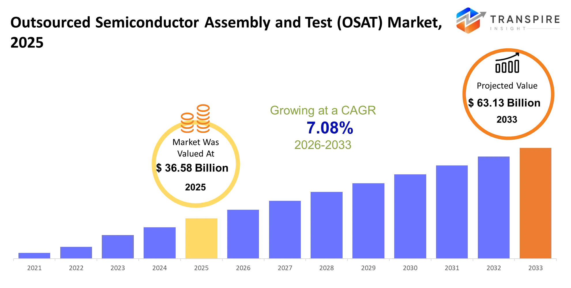
As per Transpire Insight, The Outsourced Semiconductor Assembly and Test (OSAT) Market size is estimated at USD 36.58 billion in 2025 and is anticipated to reach USD 63.13 billion by 2033, growing at a CAGR of 7.08% from 2026 to 2033.
The OSAT market enables semiconductor companies to outsource semiconductor chip assembly, packaging, and testing rather than investing in the required manufacturing facilities independently. Over the last three to five years, the industry has shifted from traditional packaging processes to advanced packaging processes designed for stacking multiple chiplets, boosting performance, and facilitating miniaturised electronic devices. The rise of artificial intelligence infrastructure, electric vehicles, and high-performance computers has increased the demand for advanced packaging and verification architecture. A major structural change in the market is moving towards chiplet architecture and 2.5D/3D integration to allow manufacturers to combine multiple dies within one package. Ongoing restrictions on the supply of semiconductors and government-supported manufacturing programmes are driving regional packaging investments. As chip designs become more complex, semiconductor manufacturers are more dependent on specialised OSAT providers to reduce manufacturing complexity, improve manufacturing flexibility, and help offset the investment costs of establishing in-house assembly and testing facilities.
Outsourced Semiconductor Assembly and Test (OSAT) Market Size & Forecast:
- Market Size 2025: USD 36.58 Billion
- Expected Market Value (2033): USD 63.13 Billion
- Forecast CAGR (2026–2033): 7.08%
- Leading Region in 2025: Asia Pacific
- Fastest Growing Region: North America
- Key Company Profiles: ASE Technology, Amkor Technology, JCET, Powertech Technology, Tongfu Microelectronics, TFME, UTAC, ChipMOS Technologies, Hana Micron, KYEC, Unisem, Carsem, Nepes, Huatian Technology, Tianshui Huatian.
Key Outsourced Semiconductor Assembly and Test (OSAT) Market Insights:
OSAT competition is moving from low-cost assembly to advanced packaging, yield control, and secure regional capacity. Organisations that are able to deliver high volumes of executions and have specific integration and testing expertise are more likely to be successful in securing complex semiconductor programmes.
- Asia Pacific accounts for 72.4% of the demand, with high wafer-fab, substrate, and OSAT concentration in Taiwan, China, Korea, and Southeast Asia.
- To double the leading-edge packaging revenue by 2027, ASE is expanding LEAP, fan-out, SiP, and chiplet capacity.
- Amkor is constructing a campus in Arizona for advanced packaging and test, and is increasing its capacity in Southeast Asia for 2.5D/3D packaging for AI and HPC customers.
- JCET is expanding the advanced packaging business in Shanghai, building up the domestic AI-chip packaging industry in China.
- Powertech Technology is investing more in memory packaging and test to meet the demand for HBM and high-bandwidth memory.
- Tongfu Microelectronics is growing its high-performance packaging and testing solutions for Chinese AI and processor designers.
- North America is the fastest-growing region with a CAGR of 10.2%, supported by localisation and demand for AI data centres, related to CHIPS.
- Europe's share is 8%, with automotive reliability, industrial semiconductors, and OSAT capacity from Portugal leading growth.
- Latin America and the Middle East & Africa account for 3% and 3.6% growth, respectively, and are reliant on electronics assembly, connectivity, and energy-sector chip demand.
- Geopolitical concentration risks and trusted supply chains are becoming more important to customers, who are increasingly looking at multi-region OSAT networks.
What are the Key Drivers, Restraints, and Opportunities in the Outsourced Semiconductor Assembly and Test (OSAT) Market?
Driver:
AI, high-performance computing, and chiplet-based designs are driving demand for advanced assembly, HBM integration, and system-level testing. The trigger is the rapid commercial deployment of AI servers and accelerators, which need 2.5D/3D packaging, silicon interposers, and chiplet interconnect validation. This raises revenue per chip because AI packages contain multiple dies, memory stacks, and large substrates, while also pushing fabless companies and IDMs to outsource specialized back-end capacity.
Restraint:
Advanced packaging remains capital- and talent-intensive. Lithography, bonding, inspection, cleanroom, and test equipment require heavy investment, while skilled process engineers and statistical quality-control specialists remain scarce, especially in North America and Europe. The constraint persists because equipment lead times, process know-how, and yield-management expertise cannot be scaled as quickly as AI demand.
Opportunity:
Regional supply-chain diversification is creating a new growth avenue for OSAT providers. Government-backed investments in the United States, Europe, Japan, and India are encouraging localised advanced-packaging ecosystems through partnerships among OSATs, foundries, and substrate suppliers. ASE’s 2025 expansion in 2.5D and 3D IC capacity demonstrates how OSATs can capture AI and HPC demand beyond traditional Asian assembly hubs. This shift reduces geographic concentration risk while supporting secure, high-value packaging capacity.
What Has the Impact of Artificial Intelligence Been on the Outsourced Semiconductor Assembly and Test (OSAT) Market?
AI is already leading the way in OSAT in the form of automated inspection, predictive maintenance, process control, and more demanding chip-testing requirements. Machine-vision systems can detect packaging defects, misaligned connections, surface anomalies, and other flaws more reliably than human inspectors. Analytics help engineers avoid process drift by catching problems early in the production cycle so that large batches of defective units can be avoided.
Predictive models compare equipment telemetry, temperature profiles, process history, and test results to predict when maintenance will be required, and thus avoid costly unplanned downtime. Yield analysis, aided by AI, can uncover recurring errors across assembly process steps, allowing manufacturers to tune bonding, material handling, and inspection thresholds accordingly. Many of these challenges are more acute with advanced packages, where more islands of chips and dense interconnects can magnify the number of failure modes. The demand for AI hardware itself is real as well, given the number of problems found in the high-performance computing processors as they get packaged and validated. Amkor's recent partnership with NVIDIA illustrates just how commercially significant advanced packaging has become for AI infrastructure.
In June 2026, TSMC and Amkor Technology signed a 10-year agreement to expand advanced semiconductor packaging and testing capacity in the United States. This partnership focuses on Arizona, combining TSMC's front-end wafer fabrication with Amkor’s back-end assembly to provide a seamless, domestic turnkey manufacturing platform for shared customers.
https://anysilicon.com/news/tsmc-and-amkor-technology-sign-10-year-u-s-advanced-packaging-agreement/
Key Outsourced Semiconductor Assembly and Test (OSAT) Market Trends:
OSAT is developing from being a volume-based back-end service to a strategic technology partner for complex chip integration. The ability to package advanced products, have access to reliable testing, and have geographically resilient production networks are key to competitive advantage.
- AI accelerators are changing the OSAT market towards 2.5D/3D integration, HBM assembly, and high-density interconnects.
- Packaging, interconnect testing and known-good-die validation are critical to product success with chiplet architectures.
- Alongside the traditional wire-bond assembly, there are faster-growing packaging technologies such as fan-out, flip-chip and panel-level packaging.
- System-level test is growing to validate thermal performance, latency, power delivery, and AI-workload performance.
- The trend of collaboration and competition is growing across advanced-packaging capacity between foundries, IDMs, and OSATs.
- The demands for reliable, high-temperature, safety-qualified packaging are growing with automotive electrification and ADAS.
- Advanced chips may be built and tested in different locations due to export control compliance and trusted-supply-chain requirements.
- Governments are investing in building capacity for packaging within the country to lessen reliance on the Asian packaging hubs.
- OSATs are investing in co-packaged optics, advanced substrates, and heterogeneous integration to meet next-generation computing needs.
Outsourced Semiconductor Assembly and Test (OSAT) Market Segmentation
By Service:
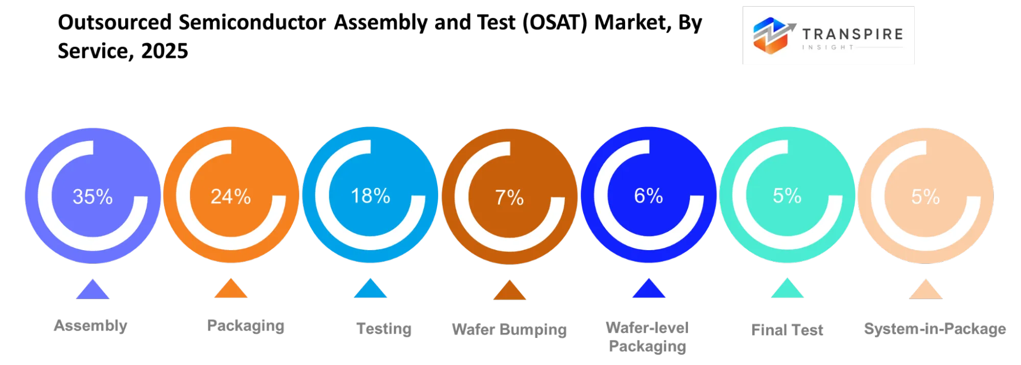
Assembly holds the largest share at 34.8%, as it converts fabricated semiconductor dies into functional components ready for integration into electronic products. Packaging accounts for 24%, followed by testing at 18%, wafer bumping at 7%, wafer-level packaging at 6%, final testing at 5%, system-in-package at 3%, and other services at 2.2%. Advanced packaging is the fastest-growing service category, with a projected 12.8% CAGR, driven by AI accelerators, high-performance computing, and chiplet integration. Wafer bumping supports advanced interconnections, while comprehensive testing helps improve yield, reliability, and performance as chip complexity increases.
By Packaging Type:
Ball grid array (BGA), quad flat no-lead (QFN), and quad flat package (QFP) formats remain important for balancing manufacturing cost, electrical performance, and reliability across established semiconductor applications. Chip-scale packages (CSP), wafer-level chip-scale packaging (WLCSP), and flip-chip technologies support smaller footprints and higher interconnect density in compact electronic devices. Meanwhile, 2.5D and 3D packaging are gaining importance in AI accelerators and high-performance computing, where integrating multiple dies improves bandwidth and processing efficiency.
By Application:
Consumer electronics supports substantial OSAT volumes through smartphones, laptops, wearables, and other connected devices that require cost-efficient packaging. Communications applications require reliable radio-frequency performance for wireless infrastructure and connectivity equipment. Automotive electronics depend on durable packaging and rigorous qualification because powertrain, driver-assistance, and vehicle-control systems operate under demanding conditions. Industrial automation, healthcare equipment, aerospace and defence systems, computing infrastructure, and other applications create additional opportunities for specialised packaging and testing designed around safety, thermal stability, and operational reliability.
By Semiconductor Type:
Analogue and power semiconductors support signal conditioning, power conversion, and energy management across industrial equipment, vehicles, and consumer electronics. Logic chips process instructions and calculations, while memory devices store the data required by computing systems and AI workloads. Microcontrollers enable embedded control in automotive and industrial applications, whereas radio-frequency (RF) chips support wireless communications. Sensors convert physical conditions into electronic signals, enabling monitoring and automation. These diverse requirements encourage OSAT providers to tailor assembly processes, packaging materials, and testing procedures to each device category.
By Technology:
Conventional packaging remains commercially important because mature semiconductor devices require dependable, cost-effective manufacturing at scale. Fan-in and fan-out technologies address different integration and footprint requirements, while flip-chip interconnects support improved electrical performance in demanding applications. Two-and-a-half-dimensional (2.5D) and three-dimensional (3D) integrated circuits enable closer integration of multiple dies, reducing interconnect distances and supporting higher bandwidth. Chiplet architectures further allow manufacturers to combine specialised processing units within one package. As AI workloads become more complex, investment in advanced packaging is expected to increase.
By End User:
Fabless semiconductor companies rely on OSAT providers because outsourcing avoids the capital expenditure required to establish dedicated assembly and testing facilities. Integrated device manufacturers (IDMs) use external capacity to supplement internal production, manage demand fluctuations, or access specialised packaging technologies. Foundries collaborate with packaging partners to provide customers with broader manufacturing solutions. Original equipment manufacturers (OEMs) and system companies benefit from supply-chain flexibility and application-specific integration. Research institutions and government organisations also use specialised services for prototype development, technology validation, and strategic semiconductor programmes, creating opportunities beyond conventional commercial production.
By Testing Type:
Wafer sort identifies defective dies before packaging, helping manufacturers avoid spending additional resources on unsuitable components. Final testing verifies whether packaged chips meet electrical and functional specifications before shipment. Burn-in testing exposes devices to controlled stress conditions to identify early failures, while reliability testing assesses performance over extended operating periods. Parametric testing measures electrical characteristics, and functional testing checks whether devices perform their intended operations. System-level testing evaluates chips under conditions closer to actual use. As AI and automotive semiconductors become more complex, comprehensive test coverage becomes increasingly important for controlling defects and protecting product reliability.
What are the Key Use Cases Driving the Outsourced Semiconductor Assembly and Test (OSAT) Market?
The core use case is advanced packaging and testing for AI accelerators and high-performance computing platforms. These products rely on assembly services, advanced packaging, and system-level testing to integrate logic dies, HBM, interposers, and chiplets; this directly supports the 34.8% assembly share and the 12.8% CAGR in advanced packaging.
Expanding applications include 5G communications, data-centre networking, automotive ADAS, power electronics, and industrial automation. Automotive and industrial chips require reliability testing, burn-in, and robust packaging, while communications devices use RF, sensor, and power semiconductors in compact packages.
Emerging use cases include co-packaged optics, chiplet-based custom processors, edge-AI modules, and domestically secured advanced-packaging supply chains. These applications connect OSATs more closely with system companies, governments, and research institutions, extending the market beyond traditional semiconductor manufacturing.
|
Report Metrics |
Details |
|
Market size value in 2025 |
USD 36.58 Billion |
|
Market size value in 2026 |
USD 39.10 Billion |
|
Revenue forecast in 2033 |
USD 63.13 Billion |
|
Growth rate |
CAGR of 7.08% from 2026 to 2033 |
|
Base year |
2025 |
|
Historical data |
2021 - 2024 |
|
Forecast period |
2026 - 2033 |
|
Report coverage |
Revenue forecast, competitive landscape, growth factors, and trends |
|
Regional scope |
United States; Canada; Mexico; United Kingdom; Germany; France; Italy; Spain; Denmark; Sweden; Norway; China; Japan; India; Australia; South Korea; Thailand; Brazil; Argentina; South Africa; Saudi Arabia; United Arab Emirates |
|
Key companies profiled |
ASE Technology, Amkor Technology, JCET, Powertech Technology, Tongfu Microelectronics, TFME, UTAC, ChipMOS Technologies, Hana Micron, KYEC, Unisem, Carsem, Nepes, Huatian Technology, Tianshui Huatian |
|
Customization scope |
Free report customization (country, regional & segment scope). Available customized purchase options to meet your exact research needs. |
|
Report Segmentation |
By Service (Assembly, Packaging, Testing, Wafer Bumping, Wafer-level Packaging, Final Test, System-in-Package, Others); By Packaging Type (BGA, QFN, QFP, CSP, WLCSP, Flip-chip, 2.5D/3D, Others); By Application (Consumer Electronics, Communications, Automotive, Industrial, Healthcare, Aerospace & Defense, Computing, Others); By Semiconductor Type (Analog, Logic, Memory, Microcontroller, Power, RF, Sensor, Others); By Technology (Conventional Packaging, Advanced Packaging, Fan-out, Fan-in, 2.5D, 3D IC, Chiplet, Others); By End User (Fabless Companies, IDMs, Foundries, OEMs, System Companies, Research Institutions, Government, Others); By Testing Type (Wafer Sort, Final Test, Burn-in, Reliability Testing, Parametric Testing, Functional Testing, System-level Testing, Others). |
Which Regions are Driving the Outsourced Semiconductor Assembly and Test (OSAT) Market Growth?
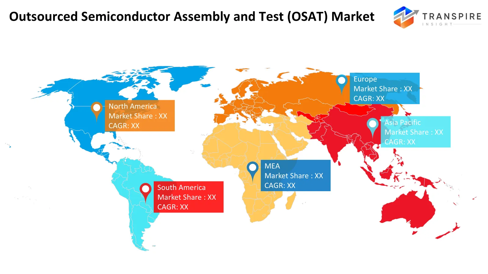
Asia Pacific dominates the OSAT market at 72.4% based on size, low cost, and proximity to the top wafer foundries, substrate makers, and consumer electronics manufacturers. Taiwan, China, Korea, Malaysia, Vietnam, and the Philippines are the key players with mature cleanroom facilities, an experienced engineering community, and captive customer bases. Government incentives, export-focused manufacturing strategies, and rising demand for AI, smartphone, and automobile components set the Asia Pacific APAC region apart.
In July 2026, ASE Technology Holding, the world's largest semiconductor packaging and testing provider, announced a massive $2 billion increase to its 2026 capital expenditure budget, raising the total cap to approximately $10.5 billion.
Europe accounts for 8% of the market, its ecosystem being more linked to automotive, industrial, and niche applications, rather than outsourced packaging volumes. This makes it stronger in terms of what is demanded from qualified automotive components, power semiconductors, and industrial electronics. The European Chips Act, as well as the national programs it spurs, aims to improve European chips' resilience and to trigger investments throughout the chain, with a focus on reliable, application-oriented packaging and testing rather than on packaging volume.
In March 2026, Silicon Box secured the Open EU Foundry (OEF) status under the European Chips Act framework for its upcoming advanced semiconductor packaging and testing facility in Novara, Italy.
North America is the fastest-growing region at a 10.2% CAGR, representing 13% of the market, driven by investments in AI infrastructure, concerns about supply-chain security, and US semiconductor policy supporting domestic advanced-packaging capacity. The growth of the Amkor Arizona campus (boosting planned investment to roughly $12 billion) is indicative. The key opportunities are AI accelerators, high-performance compute, and a closer integration of wafer fab and packaging. Latin America has a 3% share, with opportunities in diversifying the electronics supply chain. The Middle East and Africa have a 3.6% share, with future potential based on investment incentives, infrastructure, and the skills of the workforce.
In October 2026, GlobalFoundries entered into a multi-year manufacturing partnership with TSMC to fabricate silicon interposers. This agreement establishes a secure domestic supply of a critical packaging component required for TSMC's CoWoS advanced packaging ecosystem.
Who are the Key Players in the Outsourced Semiconductor Assembly and Test (OSAT) Market, and how do they compete?
Competition among providers in the Outsourced Semiconductor Assembly and Test (OSAT) market occurs through manufacturing scale, packaging tech, customer qualification, and ability to consistently produce good yields. ASE Technology competes on service integration and packaging innovation, while Amkor Technology emphasises reach and regional investment in advanced-packaging capacity. The Arizona expansion raises the planned investments to around $12b, which is indicative of the domestic supply-chain awareness and demand related to AI technology.
JCET and Tongfu Microelectronics (TFME) compete on scale and on technology for computing, communications, and automotive applications. Powertech Technology is focused on memory packaging and testing, while ChipMOS Technologies performs display-driver-IC-related testing. KYEC's specialisation is in semiconductor testing. This portfolio is commoditised, with different emphasis on scale, co-development, yield, and technology for testing and packaging, and competes by providing complex validation for customers without building dedicated facilities. UTAC, Hana Micron, Unisem, Carsem, Nepes, and Huatian Technology (Tianshui Huatian) compete on cost, regional manufacturing, and application-specific packaging, with the capacity expansion determined by customers, process reliability, and selective investment in application-specific advanced technology. Across the market, co-development and yield performance are dominating differentiators, along with facilitating scale without sacrificing quality.
Key Players are:
- ASE Technology
- Amkor Technology
- JCET
- Powertech Technology
- Tongfu Microelectronics
- TFME
- UTAC
- ChipMOS Technologies
- Hana Micron
- KYEC
- Unisem
- Carsem
- Nepes
- Huatian Technology
- Tianshui Huatian
Recent Development News
- In September 2026, Tata Electronics entered a strategic partnership with Besi to strengthen advanced semiconductor packaging capabilities at its planned ₹3-billion-dollar-equivalent investment facility in Jagiroad, Assam. The collaboration will leverage Besi’s advanced packaging equipment and technologies to accelerate facility readiness and support the development of India’s domestic OSAT ecosystem. https://www.tataelectronics.com/w/tata-electronics-and-besi-enter-strategic-partnership-to-strengthen-advanced-packaging-capabilities
- In July 2026, Micross Components announced a definitive agreement to acquire AEMtec GmbH, a provider of advanced packaging, optoelectronic modules, assembly and testing services. The acquisition is expected to expand Micross’s European footprint and strengthen its capabilities in high-reliability microelectronics for aerospace, defence, medical and industrial applications. https://www.micross.com/about-us/news-and-info/press-releases/micross-to-acquire-aemtec
- In September 2026, Kaynes Technology India announced plans to apply for a new USD 1 billion expansion project in Gujarat through its specialised semiconductor division, Kaynes Semicon. Financed under India's newly updated Semicon 2.0 government subsidy layout, this funding initiative establishes advanced co-packaged optics, chiplet integration, and multi-chip module testing ecosystems outside traditional manufacturing hubs. https://www.sahi.com/news/kaynes-technology-eyes-1-billion-osat-expansion-targets-250-300-crore-semiconductor-revenue
What Strategic Insights Define the Future of the Outsourced Semiconductor Assembly and Test (OSAT) Market?
The end game in OSAT is developing a dual-speed portfolio. While traditional assembly remains relevant for high-volume, low-cost products, it is clear that advanced packaging will soon be the path to access high-technology programs, particularly in AI and HPC. Businesses that develop early design relationships and align their investments with these customer programs by providing integrated assembly, testing, and reliability will capture higher-margin work. OEM/IDMs will look to ramp capacity before customer qualification and actual demand, leading to these potential excess costs and utilisation risks. The industry is unlikely to value geographic diversification until regional ecosystems are developed, thus increasing costs of operation. An emerging opportunity in chiplet integration, high-bandwidth memory, and panel-level packaging offers the prospect of increasing interconnect density and manufacturing efficiency to create incremental revenue. OSAT providers should invest with committed customer programs, build process-control capabilities, and invest in technologies with clear qualification pathways, without overinvesting in advanced packaging and not projecting ordinary revenues from traditional services.
Key Segmentations are:
By Service
- Assembly
- Packaging
- Testing
- Wafer Bumping
- Wafer-level Packaging
- Final Test
- System-in-Package
- Others
By Packaging Type
- BGA
- QFN
- QFP
- CSP
- WLCSP
- Flip-chip
- 2.5D/3D
- Others
By Application
- Consumer Electronics
- Communications
- Automotive
- Industrial
- Healthcare
- Aerospace & Defence
- Computing
- Others
By Semiconductor Type
- Analogue
- Logic
- Memory
- Microcontroller
- Power
- RF
- Sensor
- Others
By Technology
- Conventional Packaging
- Advanced Packaging
- Fan-out
- Fan-in
- 2.5D
- 3D IC
- Chiplet
- Others
By End User
- Fabless Companies
- IDMs
- Foundries
- OEMs
- System Companies
- Research Institutions
- Government
- Others
By Testing Type
- Wafer Sort
- Final Test
- Burn-in
- Reliability Testing
- Parametric Testing
- Functional Testing
- System-level Testing
- Others
By Regional Analysis
North America
- US
- Canada
- Mexico
Europe
- Germany
- UK
- France
- Italy
- Spain
- Russia
- Rest of Europe
Asia Pacific
- China
- Japan
- India
- South Korea
- Australia
- Rest of Asia Pacific
South America
- Brazil
- Argentina
- Rest of South America
Middle East & Africa
- UAE
- Saudi Arabia
- Qatar
- South Africa
- Rest of the Middle East & Africa
Frequently Asked Questions
Find quick answers to common questions.
The outsourced semiconductor assembly and test (OSAT) market size was valued at USD 36.58 billion in 2025 and is poised to reach USD 63.13 billion by 2033, expanding at a 7.08% CAGR.
Key segments for the outsourced semiconductor assembly and test (OSAT) market are By Service (Assembly, Packaging, Testing, Wafer Bumping, Wafer-level Packaging, Final Test, System-in-Package, Others); By Packaging Type (BGA, QFN, QFP, CSP, WLCSP, Flip-chip, 2.5D/3D, Others); By Application (Consumer Electronics, Communications, Automotive, Industrial, Healthcare, Aerospace & Defense, Computing, Others); By Semiconductor Type (Analog, Logic, Memory, Microcontroller, Power, RF, Sensor, Others); By Technology (Conventional Packaging, Advanced Packaging, Fan-out, Fan-in, 2.5D, 3D IC, Chiplet, Others); By End User (Fabless Companies, IDMs, Foundries, OEMs, System Companies, Research Institutions, Government, Others); By Testing Type (Wafer Sort, Final Test, Burn-in, Reliability Testing, Parametric Testing, Functional Testing, System-level Testing, Others).
Growth is primarily driven by AI accelerators, high-performance computing, chiplet integration, advanced packaging technologies, automotive electrification, and semiconductor supply-chain diversification.
The market is led by major manufacturers, including ASE Technology, Amkor Technology, JCET, Powertech Technology, Tongfu Microelectronics, TFME, UTAC, ChipMOS Technologies, Hana Micron, KYEC, Unisem, Carsem, Nepes, Huatian Technology, Tianshui Huatian.
Asia Pacific dominates with a 72.4% market share, supported by established semiconductor manufacturing hubs, skilled labour, integrated supplier networks, cost-efficient production, and strong electronics manufacturing demand.
Key opportunities include chiplet integration, 2.5D/3D advanced packaging, high-bandwidth memory, panel-level packaging, AI chip testing, and regional semiconductor manufacturing investments.
- ASE Technology
- Amkor Technology
- JCET
- Powertech Technology
- Tongfu Microelectronics
- TFME
- UTAC
- ChipMOS Technologies
- Hana Micron
- KYEC
- Unisem
- Carsem
- Nepes
- Huatian Technology
- Tianshui Huatian
About the Authors

Avinash Kumar
I’m Avinash Kumar, a Senior Research Analyst at Transpire Insight, with expertise in the Electronics and Semiconductor and Energy & Power industry. My work focuses on analyzing emerging technologies, market trends, industry developments, and innovation across these sectors. I specialize in transforming complex technical and market insights into clear, research-backed content that helps professionals, businesses, and decision-makers stay informed. Through continuous industry research and data-driven analysis, I strive to deliver accurate, reliable, and practical perspectives on the latest advancements shaping the semiconductor and energy landscape.

Chakradhar Khansole
Chakradhar serves as the Research Director at Transpire Insight, bringing over 8 years of experience in technology, innovation, and strategic market intelligence. He specializes in transforming complex market data into actionable business insights that enable organizations to make informed, growth-oriented decisions. Recognized for his strategic vision and analytical expertise, Chakradhar leads high-impact research initiatives, delivering comprehensive market assessments, competitive intelligence, and forward-looking industry analysis.
Recently Published Reports
-
Apr 2026
Fiber Optic Faceplates Market
Fiber Optic Faceplates Market Size, Share & Analysis Report By Type (< 300 mm2, 300-350 mm2, and > 350 mm2, By Application (Night Vision, Holographic Imaging, Medical, and Others), and Geography (North America, Europe, Asia-Pacific, Middle East and Africa, South and Central America), 2021 - 2031
-
Apr 2026
High Temperature Superconductors Market
High Temperature Superconductors Market Size, Share & Analysis Report By Type (1G HTS, and 2G HTS), By Application (Power Cable, Fault Current Limiter, and Transformer), and Geography (North America, Europe, Asia-Pacific, Middle East and Africa, South and Central America), 2021 - 2031
-
Apr 2026
Industrial Plugs and Socket Market
Industrial Plugs and Socket Market Size, Share & Analysis Report By Type (Industrial Plugs, Industrial Sockets), By Current (Up to 32 A, 32 to 125 A, Above 125 A), By Protection (Dustproof and Splash Proof, Waterproof, Explosion Proof), By End User (Heavy Industries, Oil and Gas, Chemicals and Pharmaceuticals, Power Generation, Others), and Geography (North America, Europe, Asia-Pacific, Middle East and Africa, South and Central America), 2021 - 2031
-
Apr 2026
InGaAs Avalanche Photodiodes Market
InGaAs Avalanche Photodiodes Market Size, Share & Analysis Report By Type (1100 - 1700 nm, and 1000 - 1600 nm), By Application (Missile Warning System, Muzzle Flash Detection, Wafer Defect Inspection, Laser Rangefinders, and Others), and Geography (North America, Europe, Asia-Pacific, Middle East and Africa, South and Central America), 2021 - 2031