

Japan Electrostatic Chucks Market Summary:
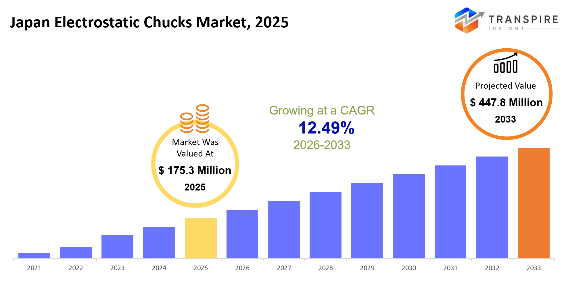
According to Transpire Insights, a detailed research report on the Japan Electrostatic Chucks Market reflects that the market was valued at approximately USD 175.3 million in 2025 and is expected to reach USD 196.5 million in 2026, further expanding to an estimated USD 447.8 million by 2033, registering a CAGR of 12.49% during 2026–2033. The market growth is driven by increasing semiconductor manufacturing activities, advanced wafer-processing requirements, and rising adoption of high-performance electrostatic chuck technologies, making it a key contributor to Japan’s semiconductor equipment development, technological innovation, advanced manufacturing capabilities, and overall market growth dynamics.
Market Snapshot
- Market Value (2025): USD 175.3 Million.
- Expected Market Value (2026): USD 196.5 Million.
- Estimated Market Value (2033): USD 447.8 Million.
- Forecast CAGR (2026–2033): 12.49%
Introduction
Japan Electrostatic Chucks Market plays a critical role in the country’s highly developed semiconductor and electronics manufacturing industry, enabling precise wafer handling in complex fabrication procedures. Electrostatic chucks are devices that utilize electrostatic forces to hold wafers and substrates securely without mechanical clamping, providing benefits in stability, surface protection, thermal control, and process accuracy. Their use is especially critical in plasma etching, deposition, lithography, wafer inspection and other high-precision semiconductor manufacturing applications. For specialized processing needs, electrostatic chucks (Coulomb-type and Johnsen-Rahbek) are utilized, with advanced ceramics enhancing durability and resistance to harsh plasma environments. Japan's strength in semiconductor equipment, precision engineering, advanced ceramics and materials science further underpin technological development. The Japan Electrostatic Chucks Market continues to be bolstered by growing demand for advanced chip manufacturing, display production, and next-generation fabrication technologies.
Key Market Highlights: -
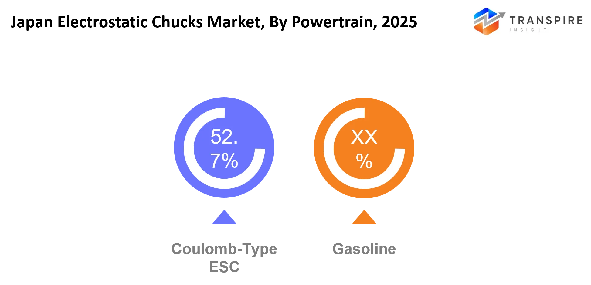
- By Type, the Coulomb Type Electrostatic dominated the market and holds approximately 57% share in 2025 and is projected to grow at a substantial CAGR during the forecast period.
- By Application, the LITHOGRAPHY SEGMENT dominated the market and holds approximately 29% share in 2025 and is projected to grow at a substantial CAGR during the forecast period.
- By Wafer Size, the 300 mm wafer segment Manufacturers segment dominated the market and holds approximately 75% share in 2025 and is projected to grow at a substantial CAGR during the forecast period.
- Semiconductor localisation efforts in Japan are supporting demand for advanced electrostatic chucks for precision wafer processing, thermal management, equipment upgrades and robust domestic semiconductor manufacturing.
How is Technology Driving Growth in the Japan Electrostatic Chucks Market?
Technological advancements in advanced ceramics, dielectric materials, thermal management and precision wafer processing are propelling the Japan Electrostatic Chucks Market. The growing use of advanced semiconductor architectures such as AI processors and memory devices is driving up demand for stable wafer clamping during etching and deposition. Next-generation ESC designs improve temperature uniformity, plasma compatibility, wafer positioning and contamination control, enabling ever more demanding fabrication processes. Also, the addition of sensors and smart process monitoring capabilities is enabling better management of chuck performance. In addition, collaboration between electrostatic chuck manufacturers, ceramic experts and semiconductor equipment companies is encouraging customized solutions for advanced-node manufacturing. The technological advances are augmenting Japan’s precision semiconductor equipment capabilities, and enabling continuous growth across the Japan Electrostatic Chucks Market.
Market Drivers
The Japan Electrostatic Chucks Market is driven by the growth of advanced semiconductor manufacturing and increasing complexity of wafer-processing needs. The rising production of AI processors, high-performance memory, 5G components and other advanced electronic devices is generating demand for precision, non-mechanical wafer clamping and effective thermal management. Japan’s efforts to revitalize its semiconductor industry and invest in domestic fabrication capacity are providing additional support to demand for high-performance semiconductor equipment and components. Meanwhile, ESC manufacturers are also making advances in ceramic materials, contamination control, temperature uniformity and chuck durability to meet demanding etching and deposition environments. The domestic supply ecosystem in Japan is also improved by the presence of established semiconductor equipment and advanced-materials companies, which boost the continued growth of the Japan Electrostatic Chucks Market.
Restrain
The Japan Electrostatic Chucks Market is confronted with challenges such as the cyclicality of the semiconductor industry, high manufacturing costs, and complex production requirements. Special ceramics, stringent contamination control, precision engineering and demanding quality standards are all necessary for high end ESCs and this increases production costs and limits scalability. Extended equipment lifecycles can also lead to longer replacement cycles and moderate recurring demand. Further, increasing competition from semiconductor equipment and component manufacturers across Asia is putting pressure on pricing and innovation. This also means that fab expansion and equipment purchases fluctuate with semiconductor capital expenditure, creating periodic uncertainty for manufacturers and suppliers of electrostatic chucks.
Analysis of Prices and Consumer Behaviour
The Japan Electrostatic Chucks Market is dominated by high-performance electrostatic chucks (68% of the total market; led by demand from the semiconductor fabrication, wafer processing and advanced-node manufacturing industries). The high-precision and advanced electrostatic chuck with superior thermal uniformity and clamping performance is expected to be 35% more expensive than other products, as the product would be manufactured using advanced ceramic materials, precision engineering and stringent quality standards. Ceramic-based electrostatic chucks account for approximately 45% of all unit sales. Their reliability in semiconductor processing and long operational life drive the sales volume. These industries account for approximately 70% of the demand of the semiconductor and advanced electronics industries. The purchasing behavior of manufacturers shows that 55% of customers consider clamping stability, thermal uniformity and product reliability as most important. 33% of the customers prefer to buy their products through bulk agreements or long term contracts to minimize their costs associated with procurement of products and to ensure a consistent source of supply to their customers in different parts of the world.
Top Companies in the Japan Electrostatic Chucks Market
- TOTO
- NGK Insulators
- Kyocera
- TOTO Advanced Ceramics
- Lam Research
- Applied Materials
- Tokyo Electron
- Entegris
- II-VI
- CoorsTek
- FM Industries
- Cast Aluminum Solutions
- Kinik
- MiCo Ceramics
- Sumitomo Electric
Japan Electrostatic Chucks Market Segmentation
The Japan Electrostatic Chucks Market share is divided into six categories: By Type, By Application, By Wafer Size, By Material, By End User, By Technology.
The Coulomb Type Electrostatic dominated the market, accounting for nearly 57% in 2025 and is expected to rise at a significant CAGR during the forecast period.
The Japan Electrostatic Chucks Market is segmented by type into coulomb type, johnsen-rahbek type, bipolar esc, monopolar esc, ceramic esc, quartz esc, silicon esc, hybrid esc. Among these, the Coulomb Type Electrostatic segment dominated the market, accounting for nearly 57% in 2025 and expected to increase at a significant CAGR during the forecast period. In 2025, the Japan Electrostatic Chucks Market was dominated by the Coulomb Type Electrostatic Chuck with a major share of nearly 57% owing to its reliable wafer clamping, accurate control, and compatibility with advanced semiconductor processing.
The LITHOGRAPHY SEGMENT dominated the market, accounting for nearly 29% in 2025, and is expected to rise at a significant CAGR during the forecast period.
The Japan Electrostatic Chucks Market is segmented by application into semiconductor etching, cvd, pvd, ion implantation, wafer inspection, lithography, cleaning, advanced packaging. Among these, PVDF the LITHOGRAPHY SEGMENT dominated the market, accounting for nearly 29% in 2025 and expected to increase at a significant CAGR during the forecast period. The Lithography segment held a dominant share of the Japan Electrostatic Chucks Market, accounting for nearly 29% in 2025. The dominance is attributed to the requirement of precise positioning of wafers and stringent alignment requirements in advanced semiconductor fabrication processes.
The 300 mm wafer segment dominated the market, accounting for nearly 75% in 2025 and is expected to rise at a significant CAGR during the forecast period.
The Japan Electrostatic Chucks Market is segmentedby wafer size into 150 mm, 200 mm, 300 mm, 450 mm, small-diameter, large-diameter, specialty wafers, custom sizes. Among these, the 300 mm wafer segment dominated the market, accounting for nearly 75% in 2025 and expected to increase at a significant CAGR during the forecast period. The advanced-node chip production, increased wafer throughput, better process efficiency and strict demands for semiconductor manufacturing resulted in the domination of the 300 mm wafer segment.
Future Market Trends for the Japan Electrostatic Chucks Market: -
Smart ESC Integration: Intelligent sensors and real-time monitoring will improve wafer temperature control, clamping stability, predictive maintenance and process optimization in advanced semiconductor fabrication.
Advanced Ceramic Materials: High-performance AlN, Al2O3, and engineered dielectric materials will improve thermal conductivity, plasma resistance, durability and reliability across advanced wafer processing applications.
Multi-Zone Thermal Management: Multiple-zone heaters, embedded temperature sensors and localized thermal control will allow for improved wafer temperature uniformity, minimizing process variations and enabling advanced node fabrication.
Recent Development
In August 11, 2026 – TOTO’s Expansion of Electrostatic Chucks: TOTO expanded its market share in Japan’s Electrostatic Chucks Market with advanced ceramic solutions for precision wafer handling and semiconductor etching applications.
In September 02, 2026 – Japan Market Development: Japanese electrostatic chuck manufacturers are speeding up development of high-precision and energy-efficient solutions to meet the needs of AI, 5G, IoT and next-generation semiconductor manufacturing.
In August 07, 2026 – Smart Technology Integration: Japan’s electrostatic chuck industry has advanced in integrating smart-factory with digital monitoring, intelligent thermal management and energy-efficient technologies for more complex semiconductor fabrication processes.
Market Segmentation
This study forecasts revenue at Japan, regional and country levels from 2020 to 2033. Transpire Insights has segmented the Japan Electrostatic Chucks Market based on the below-mentioned segments:
Japan Electrostatic Chucks Market, By Type
- Coulomb Type
- Johnsen-Rahbek Type
- Bipolar ESC
- Monopolar ESC
- Ceramic ESC
- Quartz ESC
- Silicon ESC
- Hybrid ESC
Japan Electrostatic Chucks Market, By Application
- Semiconductor Etching
- CVD
- PVD
- Ion Implantation
- Wafer Inspection
- Lithography
- Cleaning
- Advanced Packaging
Japan Electrostatic Chucks Market, By Wafer Size
- 150 mm
- 200 mm
- 300 mm
- 450 mm
- Small-Diameter
- Large-Diameter
- Specialty Wafers
- Custom Sizes
Japan Electrostatic Chucks Market, By Material
- Aluminum Oxide
- Aluminum Nitride
- Quartz
- Silicon Carbide
- Silicon
- Yttria
- Ceramic Composites
- Other Materials
Japan Electrostatic Chucks Market, By End User
- Semiconductor Foundries
- IDMs
- Memory Manufacturers
- Equipment OEMs
- Research Institutes
- OSATs
- Compound Semiconductor Manufacturers
- LITHOGRAPHY SEGMENT Manufacturers
Japan Electrostatic Chucks Market, By Technology
- Single-Wafer
- Multi-Zone
- Temperature-Controlled
- RF-Compatible
- High-Temperature
- Cryogenic
- High-Voltage
- Smart ESC
Frequently Asked Questions
Find quick answers to common questions.
Advanced semiconductor manufacturing, AI processors, memory devices, and precision wafer processing are driving demand for high-performance electrostatic chuck technologies.
The 300 mm wafer segment dominates, supported by advanced-node production, higher throughput, process efficiency, and widespread adoption across semiconductor fabs.
Coulomb-type ESCs lead due to stable wafer clamping, precise control, low leakage, reliable release, and compatibility with advanced semiconductor processes.
Lithography leads because electrostatic chucks provide precise wafer positioning, uniform clamping, thermal stability, and alignment control required for advanced fabrication.
Future growth will emphasize smart ESCs, advanced ceramics, multi-zone thermal control, predictive monitoring, and energy-efficient solutions for advanced-node fabrication requirements.
- TOTO
- NGK Insulators
- Kyocera
- TOTO Advanced Ceramics
- Lam Research
- Applied Materials
- Tokyo Electron
- Entegris
- II-VI
- CoorsTek
- FM Industries
- Cast Aluminum Solutions
- Kinik
- MiCo Ceramics
- Sumitomo Electric
About the Authors

Avinash Kumar
I’m Avinash Kumar, a Senior Research Analyst at Transpire Insight, with expertise in the Electronics and Semiconductor and Energy & Power industry. My work focuses on analyzing emerging technologies, market trends, industry developments, and innovation across these sectors. I specialize in transforming complex technical and market insights into clear, research-backed content that helps professionals, businesses, and decision-makers stay informed. Through continuous industry research and data-driven analysis, I strive to deliver accurate, reliable, and practical perspectives on the latest advancements shaping the semiconductor and energy landscape.

Chakradhar Khansole
Chakradhar serves as the Research Director at Transpire Insight, bringing over 8 years of experience in technology, innovation, and strategic market intelligence. He specializes in transforming complex market data into actionable business insights that enable organizations to make informed, growth-oriented decisions. Recognized for his strategic vision and analytical expertise, Chakradhar leads high-impact research initiatives, delivering comprehensive market assessments, competitive intelligence, and forward-looking industry analysis.
Recently Published Reports
-
Apr 2026
Fiber Optic Faceplates Market
Fiber Optic Faceplates Market Size, Share & Analysis Report By Type (< 300 mm2, 300-350 mm2, and > 350 mm2, By Application (Night Vision, Holographic Imaging, Medical, and Others), and Geography (North America, Europe, Asia-Pacific, Middle East and Africa, South and Central America), 2021 - 2031
-
Apr 2026
High Temperature Superconductors Market
High Temperature Superconductors Market Size, Share & Analysis Report By Type (1G HTS, and 2G HTS), By Application (Power Cable, Fault Current Limiter, and Transformer), and Geography (North America, Europe, Asia-Pacific, Middle East and Africa, South and Central America), 2021 - 2031
-
Apr 2026
Industrial Plugs and Socket Market
Industrial Plugs and Socket Market Size, Share & Analysis Report By Type (Industrial Plugs, Industrial Sockets), By Current (Up to 32 A, 32 to 125 A, Above 125 A), By Protection (Dustproof and Splash Proof, Waterproof, Explosion Proof), By End User (Heavy Industries, Oil and Gas, Chemicals and Pharmaceuticals, Power Generation, Others), and Geography (North America, Europe, Asia-Pacific, Middle East and Africa, South and Central America), 2021 - 2031
-
Apr 2026
InGaAs Avalanche Photodiodes Market
InGaAs Avalanche Photodiodes Market Size, Share & Analysis Report By Type (1100 - 1700 nm, and 1000 - 1600 nm), By Application (Missile Warning System, Muzzle Flash Detection, Wafer Defect Inspection, Laser Rangefinders, and Others), and Geography (North America, Europe, Asia-Pacific, Middle East and Africa, South and Central America), 2021 - 2031