

Germany EDA Software Market Summary
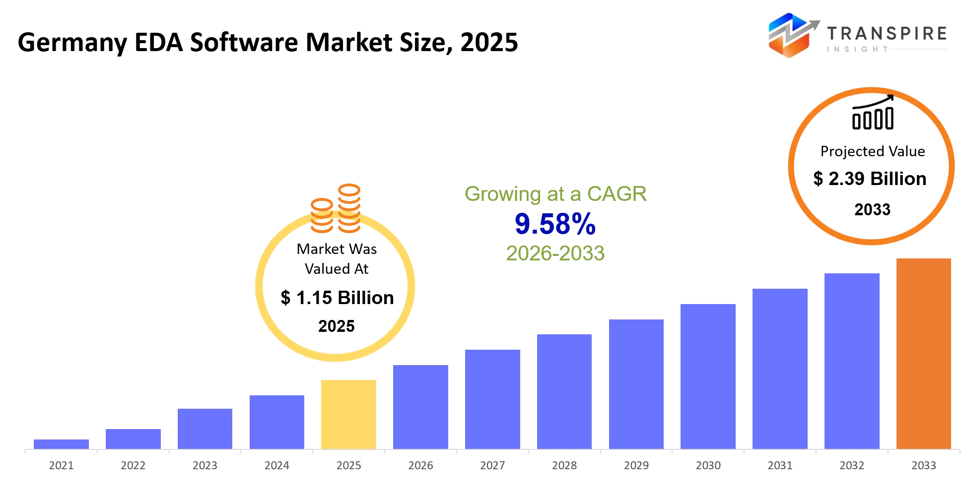
As per Transpire Insight Analysis the Germany EDA Software Market size is estimated at USD 1.15 Billion in 2025 and is anticipated to reach USD 2.39 Billion by 2033, growing at a CAGR of 9.58% from 2026 to 2033.
In the Germany EDA Software Market, companies support the design, checking, and refinement of semiconductor chips and electronic systems that keep getting more complex. These tools get used across automotive, industrial automation, telecommunications, and also aerospace manufacturing. Engineering groups lean on these kinds of software platforms to cut down on design mistakes, shrink the development time, and validate advanced integrated circuits prior to production, so manufacturers can manage their costs while still meeting rigid performance and safety requirements. Over the last five years, the whole market has been moving toward cloud- enabled collaborative design surroundings, plus AI-assisted automation, as semiconductor architectures have become more elaborate and tightly coupled. The global semiconductor supply chain troubles during 2020–2022 basically sped up investment in nearby chip creation and design know-how across Europe. In Germany, as automotive and industrial manufacturers expand work on software defined vehicles, power electronics, and AI processors, engineering organizations are adopting design automation tools earlier, in the product development timeline. This tends to raise the take from software licensing, verification, and simulation revenues too ,as these projects scale up.
Germany EDA Software Market Size & Forecast:
- Germany EDA Software Market Size 2025: USD 1.15 Billion
- Expected Market Value 2033: USD 2.39 Billion
- Forecast CAGR: 9.58%
- Key Profile: Synopsys, Cadence Design Systems, Siemens EDA, Ansys, Keysight Technologies, Altium, Zuken, Dassault Systèmes, Autodesk, Silvaco, Altair Engineering, Mentor Graphics, Xilinx (AMD), Intel, MathWorks.
Key Market Insights
- Regional Analysis: Southern Germany basically led the Germany EDA Software Market with around 42% share in 2025, and that was backed by Bavaria plus Baden-Württemberg cluster activity in semiconductors and automotive too.
- Regional Growth: Eastern Germany is expected to grow the quickest through 2033, mostly because Dresden keeps expanding its semiconductor ecosystem, alongside new wafer fabrication investments and such.
- Product Segment: Verification software took nearly 29% market share in 2025, whereas simulation software stayed the second-largest category, as chip complexity keeps climbing.
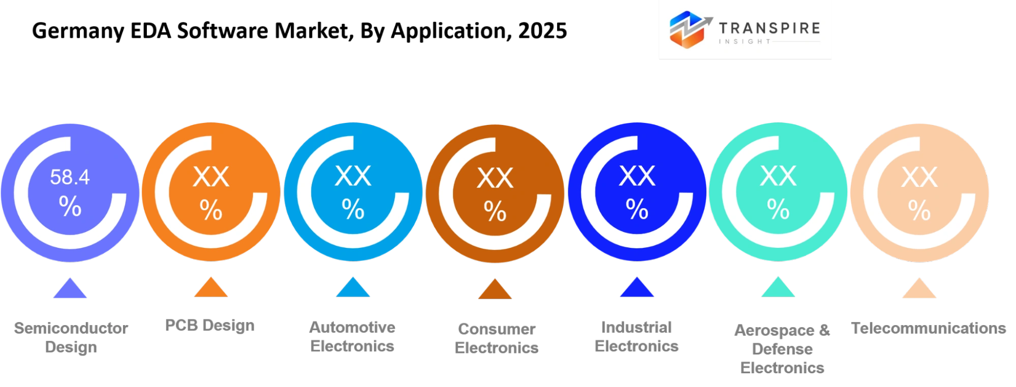
- Application & End User: Semiconductor design made up roughly 38% of total demand, while semiconductor companies contributed close to 40% of the overall software spend during 2025, in general.
- Competitive Landscape: Synopsys, Cadence Design Systems, Siemens EDA, Ansys, and Keysight Technologies are still pushing harder on their positions, using AI driven design automation, cloud teamwork, strategic partnerships, and digital validation technologies.
What are the Key Drivers, Restraints, and Opportunities in the Germany EDA Software Market?
Driver: The main growth driver seems to come from Germany’s quick, sort of rapid expansion of semiconductor design know-how, which supports automotive electrification, industrial automation, and also advanced communication tech. The European Chips Act, plus other related semiconductor investment programs, basically pushed more design work inside the region, while also lowering reliance on overseas supply lines. As design complexity keeps rising, engineering groups are being forced to bring sophisticated verification, simulation, and physical layout software earlier into the cycle. That move tends to increase recurring income from software licensing, consulting, and maintenance, and it also helps boost first-pass silicon success rates.
Restraint: On the other side, implementation expenses are high and there’s still a real shortage of seasoned chip design engineers, so it’s not just a temporary hiccup. Advanced EDA platforms need specific expertise, lots of training, and quite a bit of computing infrastructure. Smaller design firms, and even research organizations sometimes delay software upgrades because the real deployment cost ends up going past the license fee, into hardware provisioning workflow integration, and workforce development. So these obstacles end up slowing adoption, and they keep revenue growth from really moving for smaller companies.
Opportunity: For opportunities, AI accelerator development automotive chip innovation and Europe’s broader, homegrown semiconductor manufacturing ecosystem look like a strong long-term tailwind. Places like Dresden, Munich, and other tech hubs still keep pulling fabrication, and R&D investment, and all of that tends to need advanced design automation. Cloud-native EDA platforms alongside AI-assisted verification will likely broaden software uptake by cutting development time, and improving engineering output, at least that’s the direction the market is going.
What Has the Impact of Artificial Intelligence Been on the Germany EDA Software Market?
Artificial intelligence has changed electronic design automation in a real way, cutting down the engineering load across chip design, verification, timing analysis , and physical layout optimization. With these AI methods, the process can kind of „see“ design issues on its own, like spotting design rule violations, improving routing choices, suggesting circuit architectures, and sorting verification scenarios in a way that used to take weeks of manual work. Machine learning models moreover help anticipate manufacturing defects, estimate power use, and tune thermal behavior before fabrication even starts, so teams can avoid expensive silicon rework.
There’s also the whole analytics side that tightens up operational efficiency by hunting for bottlenecks in design workflows and then assigning computing resources across simulation runs automatically. Some major vendors now bundle generative AI features that speed up code generation, documentation, and even help refine hardware description language settings, which ends up shortening product timelines by about 20% to 30% in certain engineering streams. AI-driven verification can also raise the odds of first-pass success while trimming down the overall verification workload.
Even with all that, broad adoption is still kind of held back by the heavy compute demands of AI-enabled workflows and by the need for large quantities of proven, historical design data. If an organization has smaller legacy datasets they often get weaker model accuracy, so human experience and engineering supervision stay important across the full design process.
Key Market Trends
- AI assisted circuit optimization really took off after 2022, kind of enabling faster physical design closure, and also cutting down on those repetitive engineering bits across really advanced semiconductor projects, too.
- Cloud native design platforms got a lot more traction as distributed engineering teams grew, and people started collaborating on chip development across multiple centers, not just one place.
- Automotive semiconductor programs also shifted toward software defined vehicle architectures, so naturally there was more money going into verification, functional safety, and mixed signal design software.
- After 2023 , advanced packaging technologies became a bigger design priority, which then pushed wider use of multi die simulation and heterogeneous integration tools , sort of as a standard expectation.
- Semiconductor companies began allocating even larger budgets to functional verification, because verification workloads now make up almost 70% of the total chip development effort.
- Digital twin technologies slowly moved into electronic system development, helping with thermal simulation, reliability analysis, and lifecycle optimization before manufacturing even starts.
- Synopsys Cadence Design Systems Siemens EDA, and Ansys also expanded AI powered automation features, to boost day to day engineering productivity , and shorten overall product development schedules.
- FPGA development tools saw stronger adoption as industrial automation and edge AI applications demanded more flexible hardware acceleration platforms.
- Open design ecosystems plus standardized IP integration reduced development time while still supporting collaboration between semiconductor companies automotive suppliers and research institutions.
- And cybersecurity focused hardware verification became more visible too, since connected automotive, industrial, and telecommunications devices need stronger protection against hardware level vulnerabilities.
Germany EDA Software Market Segmentation
By Product Type
Verification Software is kind of leading the way since advanced semiconductor designs really do need a lot of functional validation work before fabrication. Simulation Software together with IC Physical Design Software stays crucial for tuning chip performance , managing power usage and making sure manufacturing is ready. PCB Design Software still supports electronics development across automotive, industrial automation, and telecommunications too. IP Design Tools help shrink the development time by using reusable intellectual property blocks , which is honestly a big deal.
FPGA Design Tools keep picking up momentum as edge computing, artificial intelligence, and industrial control systems move toward programmable hardware. Electronic System Design Tools make it easier to line up hardware with software for electronic products that are getting more complicated. The Others category includes specialized solutions for analog mixed-signal , RF and custom design workflows, they cover those more niche engineering requirements that don’t fit neatly elsewhere. In every category, product innovation will keep boosting design accuracy while also trimming down development cycles.
By Deployment
On-Premise deployment keeps going strong and still serves organizations dealing with extremely confidential semiconductor designs, mostly because having internal infrastructure means more control over intellectual property and regulatory compliance. Meanwhile Cloud-Based deployment has been growing, sort of steadily, because engineering teams start asking for scalable computing resources for verification and simulation. Then hybrid environments show up as a middle path, they try to bring security along with more flexible processing capacity for those heavier design projects. SaaS solutions, by the way, make the whole software update part easier and they also cut down on the amount of infrastructure management someone has to handle.
Private Cloud environments tend to pull in big semiconductor companies that need dedicated computing resources and stricter security controls, pretty straight forward. Public Cloud adoption also keeps expanding, especially among smaller organizations that want less capital investment and a faster rollout timeline. The “Others” category covers more customized deployment architectures, like for research laboratories, government projects, and those highly specialized engineering environments. Overall deployment flexibility is going to stay a key buying factor as collaborative chip development keeps increasing.
By Application
Semiconductor Design ends up holding the biggest share, because advanced integrated circuits need pretty sophisticated design automation, throughout both development and verification. PCB Design supports the building of electronic systems across multiple manufacturing industries , while also boosting layout precision and generally lowering production mistakes. Automotive Electronics keeps growing fast with electric vehicles, autonomous driving tech , and improved driver assistance capabilities. Consumer Electronics stays fairly steady in terms of software utilization, since makers roll out devices that are more compact and energy savvy.
Industrial Electronics leans on automation, robotics, and smart factory investments, which in turn depend on dependable electronic control platforms. Aerospace & Defense Electronics really needs high accuracy in verification plus safety validation for mission critical hardware. Telecommunications keeps moving forward too , using 5G infrastructure, networking equipment, and high speed communication processors. The Others bucket covers healthcare electronics, renewable energy equipment, and specialized embedded systems that back different engineering needs .
By End User
Semiconductor Companies stay the biggest end-user group ,because integrated circuit development needs ongoing money and attention toward verification, simulation, and physical design tooling . Electronics Manufacturers, on the other hand depend on advanced engineering software to help raise product quality while also cutting down development hours across a bunch of electronic devices. Automotive OEMs keep doubling down on software adoption because vehicle electronics get more complex and software-defined architectures keep showing up and spreading. Research Institutes back innovation through advanced semiconductor research, prototype building, and more academic cooperation .
Defense Organizations need secure electronic design environments, that must meet tight reliability requirements plus cybersecurity standards for mission critical uses. Telecom Equipment Manufacturers count on engineering tools for networking processors, communications infrastructure, and high-speed connectivity solutions . In the Others bucket you usually find medical device manufacturers, industrial automation suppliers, and tech startups that keep expanding electronic product development efforts. Broad industry participation keeps the long term software demand more stable too.
By Enterprise Size
Large Enterprises take the biggest share of software spending, mainly because huge semiconductor development programs need full on design, verification, and simulation platforms. Medium Enterprises keep pushing their software budget too, in order to boost engineering productivity and keep up in those niche semiconductor arenas. Small Enterprises are moving more and more toward subscription based licensing models, which trims the upfront spend while making advanced engineering capabilities easier to reach. Startups tend to lean on adaptable software platforms to speed up innovation across artificial intelligence, automotive electronics, and embedded systems .
Cloud deployment, along with scalable licensing models, is still making software easier to obtain for organizations that have limited engineering resources. Venture capital money, plus government backed semiconductor initiatives, also helps technology startups build stronger product development capabilities. The Others bucket covers consulting outfits, contract design service providers, and shared engineering organizations that support semiconductor development across several industries. Overall , these flexible licensing strategies should keep widening software adoption.
What are the Key Use Cases Driving the Germany EDA Software Market?
Semiconductor design still looks like the main thing, because advanced processors, automotive chips, and power management devices all need careful layout, plus verification, and simulation before any fabrication stuff happens. Engineering teams end up leaning on electronic design automation platforms to cut down on expensive design rework, while still hitting the tight performance, safety, and manufacturing goals that everyone talks about.
At the same time, automotive electronics and industrial automation keep showing up as fast-growing applications. Electric vehicle makers, robotics suppliers, and telecommunications equipment producers depend on modern design software to sanity check complicated electronic systems, boost reliability, and end up with shorter development cycles before they reach commercial production.
Newer use cases are also coming in, like AI accelerator chips, quantum computing hardware, silicon photonics, and advanced heterogeneous packaging technologies. With growing investment across European semiconductor manufacturing and research sites, adoption of next-generation design automation platforms is likely to spread more through the whole forecast period.
|
Report Metrics |
Details |
|
Market size value in 2025 |
USD 1.15 Billion |
|
Market size value in 2026 |
USD 1.26 Billion |
|
Revenue forecast in 2033 |
USD 2.39 Billion |
|
Growth rate |
CAGR of 9.58% from 2026 to 2033 |
|
Base year |
2025 |
|
Historical data |
2021 - 2024 |
|
Forecast period |
2026 - 2033 |
|
Report coverage |
Revenue forecast, competitive landscape, growth factors, and trends |
|
Regional scope |
Germany |
|
Key company profiled |
Synopsys, Cadence Design Systems, Siemens EDA, Ansys, Keysight Technologies, Altium, Zuken, Dassault Systèmes, Autodesk, Silvaco, Altair Engineering, Mentor Graphics, Xilinx (AMD), Intel, MathWorks. |
|
Customization scope |
Free report customization (country, regional & segment scope). Avail customized purchase options to meet your exact research needs. |
|
Report Segmentation |
By Product Type (IC Physical Design Software, PCB Design Software, Verification Software, Simulation Software, IP Design Tools, FPGA Design Tools, Electronic System Design Tools, Others); By Deployment (Cloud-Based, On-Premise, Hybrid, SaaS, Private Cloud, Public Cloud, Others); By Application (Semiconductor Design, PCB Design, Automotive Electronics, Consumer Electronics, Industrial Electronics, Aerospace & Defense Electronics, Telecommunications, Others); By End User (Semiconductor Companies, Electronics Manufacturers, Automotive OEMs, Research Institutes, Defense Organizations, Telecom Equipment Manufacturers, Others); By Enterprise Size (Large Enterprises, Medium Enterprises, Small Enterprises, Startups, Others). |
Which Regions are Driving the Germany EDA Software Market Growth?
Southern Germany stays pretty much the leading regional market, pushed forward by Bavaria and Baden-Württemberg where global semiconductor firms , automotive OEMs , research institutes and engineering software providers sit inside a tightly woven innovation ecosystem that’s kinda hard to separate in practice. Munich , Stuttgart and the nearby technology corridors get a real boost from federal and state support, for example semiconductor research, advanced manufacturing and Industry 4.0 moves. Because universities, chip designers , car makers and software vendors work close together, product development speeds up, and at the same time demand becomes more consistent for advanced electronic design automation tools . This mix of design know-how, R&D money, and industrial output keeps strengthening the region’s position in software uptake and in commercial revenue.
Western Germany comes next as the second-largest contributor, but the growth is a bit different than what you see in the southern cluster. North Rhine-Westphalia has a diversified industrial base, with telecommunications, industrial electronics , automation equipment, and enterprise software development in the mix, rather than leaning mostly on semiconductor manufacturing. Steady industrial investment, ongoing digital transformation , and the longer-term upgrading of factories , all together generate dependable needs for simulation, PCB design, and verification software. In short, economic resilience plus wider industrial variety helps keep software spending steady even when semiconductor investment cycles wobble.
Eastern Germany is anticipated to show the quickest growth between 2026 and 2033. The main driver is Saxony, where the semiconductor ecosystem keeps expanding around Dresden.
Who are the Key Players in the Germany EDA Software Market and How Do They Compete?
Competition stays fairly concentrated , mainly because advanced electronic design automation platforms need decades of algorithm work, tight cooperation with semiconductor foundries ,and a lot of deep verification knowhow. In practice the differentiators have shifted away from pure software pricing toward things like technology leadership, AI driven automation, verification accuracy, cloud scale , and support for new process nodes. Even so, the well-known vendors keep pushing their broader ecosystems via partnerships with foundries, semiconductor manufacturers, and cloud infrastructure providers while also growing AI features across the whole design lifecycle.
Synopsys sets itself apart with broad silicon to systems engineering platforms that bring chip design, verification, simulation, and multiphysics analysis together in one place. Lately, collaborations with TSMC have broadened AI powered design flows , plus certified backing for advanced process technologies so users can speed up next generation AI chip development.
Cadence Design Systems leans into AI assisted design automation, autonomous engineering workflows, and ongoing collaboration with top semiconductor foundries. Their continual investment in agentic AI capabilities , along with process optimization improvements, helps boost throughput for system-on-chip projects that keep getting more complex over time.
Siemens EDA blends semiconductor design automation with digital engineering, simulation, and industrial software functions, which tends to matter a lot for automotive and manufacturing audiences. Its collaboration with TSMC on AI enabled design automation and certified support for advanced process nodes also helps reinforce its competitive standing in cutting edge semiconductor design.
Company List
- Synopsys
- Cadence Design Systems
- Siemens EDA
- Ansys
- Keysight Technologies
- Altium
- Zuken
- Dassault Systèmes
- Autodesk
- Silvaco
- Altair Engineering
- Mentor Graphics
- Xilinx (AMD)
- Intel
- MathWorks
Recent Development News
In April 2026, Synopsys announced a partnership with TSMC to deliver AI-powered EDA flows, certified IP, and advanced design solutions for next-generation semiconductor technologies. The collaboration strengthens AI chip development and accelerates advanced-node semiconductor design.
Source: https://investor.synopsys.com
In April 2026, Siemens EDA expanded its collaboration with TSMC to advance AI-powered semiconductor design automation and achieved multiple certifications for TSMC's latest process technologies. The partnership enhances productivity across advanced chip design workflows.
Source: https://news.siemens.com
In March 2026, Synopsys launched its Multiphysics Fusion technology and introduced new AI-powered design, verification, and simulation solutions following the Ansys integration. The launch broadens silicon-to-systems engineering capabilities for AI-driven semiconductor development.
Source: https://investor.synopsys.com
What Strategic Insights Define the Future of the Germany EDA Software Market?
The Germany EDA software market seems like it is moving , pretty clearly toward AI- assisted engineering, cloud native design environments and integrated silicon to systems development, even as semiconductor architectures get more intricate and automotive electronics keep evolving into software defined platforms. The biggest long term driver , in my view, is Europe’s push to grow home based semiconductor design and manufacturing capability via strategic public and private investment. There is also a quieter kind of worry here: the market still relies on a handful of global EDA suppliers, which can create concentration risk for pricing, for innovation, and for software interoperability. On the opportunity side, things are picking up fast with chiplet architectures and heterogeneous 3D packaging, where advanced design automation, multiphysics simulation, and verification tools will be required, not just “nice to have”. Companies should broaden their AI enabled engineering capabilities, but also tighten partnerships with semiconductor foundries, cloud providers and regional research organizations to grab the next wave of high value semiconductor design work.
Germany EDA Software Market Report Segmentation
By Product Type
- IC Physical Design Software
- PCB Design Software
- Verification Software
- Simulation Software
- IP Design Tools
- FPGA Design Tools
- Electronic System Design Tools
- Others
By Deployment
- Cloud-Based
- On-Premise
- Hybrid
- SaaS
- Private Cloud
- Public Cloud
- Others
By Application
- Semiconductor Design
- PCB Design
- Automotive Electronics
- Consumer Electronics
- Industrial Electronics
- Aerospace & Defense Electronics
- Telecommunications
- Others
By End User
- Semiconductor Companies
- Electronics Manufacturers
- Automotive OEMs
- Research Institutes
- Defense Organizations
- Telecom Equipment Manufacturers
- Others
By Enterprise Size
- Large Enterprises
- Medium Enterprises
- Small Enterprises
- Startups
- Others
Frequently Asked Questions
Find quick answers to common questions.
The expected Germany EDA Software Market size for the market will be USD 2.39 Billion in 2033.
Key segments for the Germany EDA Software Market are By Product Type (IC Physical Design Software, PCB Design Software, Verification Software, Simulation Software, IP Design Tools, FPGA Design Tools, Electronic System Design Tools, Others); By Deployment (Cloud-Based, On-Premise, Hybrid, SaaS, Private Cloud, Public Cloud, Others); By Application (Semiconductor Design, PCB Design, Automotive Electronics, Consumer Electronics, Industrial Electronics, Aerospace & Defense Electronics, Telecommunications, Others); By End User (Semiconductor Companies, Electronics Manufacturers, Automotive OEMs, Research Institutes, Defense Organizations, Telecom Equipment Manufacturers, Others); By Enterprise Size (Large Enterprises, Medium Enterprises, Small Enterprises, Startups, Others).
Major Germany EDA Software Market players are Synopsys, Cadence Design Systems, Siemens EDA, Ansys, Keysight Technologies, Altium, Zuken, Dassault Systèmes, Autodesk, Silvaco, Altair Engineering, Mentor Graphics, Xilinx (AMD), Intel, MathWorks.
The Germany EDA Software Market size is USD 1.15 Billion in 2025.
The Germany EDA Software Market CAGR is 9.58% from 2026 to 2033.
- Synopsys
- Cadence Design Systems
- Siemens EDA
- Ansys
- Keysight Technologies
- Altium
- Zuken
- Dassault Systèmes
- Autodesk
- Silvaco
- Altair Engineering
- Mentor Graphics
- Xilinx (AMD)
- Intel
- MathWorks
About the Authors

Mayur Shinde
I am Mayur Shinde, a Senior Research Analyst at Transpire Insight, specializing in the Automotive & Transportation and Information & Communication Technology (ICT) Industry. My work focuses on analyzing emerging market trends, technological advancements, competitive landscapes, and industry developments to deliver accurate, data-driven insights. I am passionate about transforming complex market information into clear, actionable content that helps businesses, professionals, and decision-makers stay informed and make confident strategic decisions.

Chakradhar Khansole
Chakradhar serves as the Research Director at Transpire Insight, bringing over 8 years of experience in technology, innovation, and strategic market intelligence. He specializes in transforming complex market data into actionable business insights that enable organizations to make informed, growth-oriented decisions. Recognized for his strategic vision and analytical expertise, Chakradhar leads high-impact research initiatives, delivering comprehensive market assessments, competitive intelligence, and forward-looking industry analysis.
Recently Published Reports
-
Apr 2026
3D Optical Profiler Market
3D Optical Profiler Market Size, Share & Analysis Report By Type (Desktop 3D Optical Profiler, and Portable 3D Optical Profiler), By Technology (Confocal Technology, and White Light Interference), By End-Use Industry (Manufacturing, Research Institutions, Automotive, Aerospace and Defense, Medical Devices, and Other), and Geography (North America, Europe, Asia-Pacific, Middle East and Africa, South and Central America), 2021 - 2031
-
Apr 2026
Depth Sensor Market
Depth Sensor Market Size, Share & Analysis Report By Type (Infrared Depth Sensors, Time-of-Flight (ToF) Sensors, Stereo Vision Sensors, Structured Light Sensors, Ultrasonic Depth Sensors), By Application (Automotive, Robotics, Gaming, Consumer Electronics, Industrial Automation, Healthcare, Security & Surveillance, Others), By End Users (Automotive Manufacturers, Consumer Electronics Companies, Healthcare Providers, Industrial Companies, Security Agencies, Gaming Companies, Robotics Companies, Others), and Geography (North America, Europe, Asia-Pacific, Middle East and Africa, South and Central America), 2021 – 2031
-
Apr 2026
Digital Manufacturing Market
Digital Manufacturing Market Size, Share & Analysis Report By Component (Hardware, Software, and Services), By Technology (Robotics, 3D Printing, Internet of Things (IoT), and Others), By Application (Automotive and Transportation, Aerospace and Defense, Consumer Electronics, Industrial Machinery, and Others), By Process Type (Computer-Based Designing, Computer-Based Simulation, Computer 3D Visualization, Analytics, and Others), and Geography (North America, Europe, Asia-Pacific, Middle East and Africa, South and Central America), 2021 – 2031
-
Apr 2026
Digital Visa Services Market
Digital Visa Services Market Size, Share & Analysis Report By Type (Individual Travelers, Group Travelers), By Application (Tourism, Business Travel, Others), and Geography (North America, Europe, Asia-Pacific, Middle East and Africa, South and Central America), 2021 – 2031