
Advanced Probe Card and Wafer Probing Test Systems Market Summary:
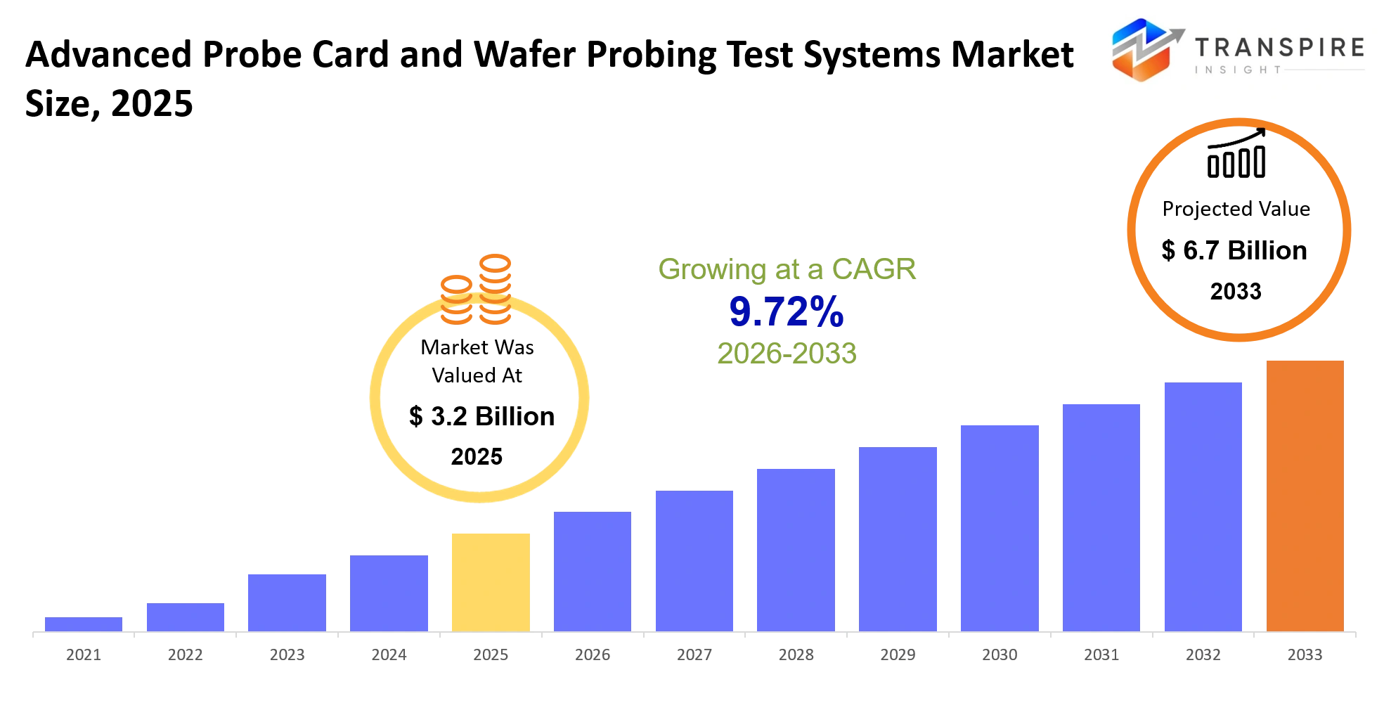
As per Transpire Insight Analysis, the Advanced Probe Card and Wafer Probing Test Systems Market size is estimated at USD 3.2 Billion in 2025 and is anticipated to reach USD 6.7 Billion by 2033, growing at a CAGR of 9.72%from 2026 to 2033. Growth will be fuelled by the rise in semiconductor manufacturing output, demand for AI and automotive semiconductors, and increased deployment of high-end wafer testing technology.
The Advanced Probe Card and Wafer Probing Test Systems Market is very important for making semiconductors. It makes sure that the wafers and circuits are tested correctly before they are put together. These tests help the people who make them find the problems early, make more of them and deal with the fact that the chips are getting more complicated.
The Advanced Probe Card and Wafer Probing Test Systems Market has changed a lot in the past few years. Now people use Advanced Probe Card and Wafer Probing Test Systems that have machines and artificial intelligence to help with the tests. They also use machines that can check things automatically to make sure the Advanced Probe Card and Wafer Probing Test Systems work well for things like intelligence, car electronics and fast computers. Many new places that make semiconductors are being built around the world. This means that people are investing money in equipment that can test the wafers very precisely. As the chips get smaller and more complicated, the people who make them need Advanced Probe Card and Wafer Probing Test Systems that're faster, more reliable and more accurate. This is why more and more people in the semiconductor industry are using the Advanced Probe Card and Wafer Probing Test Systems.
Advanced Probe Card and Wafer Probing Test Systems Market Size & Forecast:
- Market Size 2025: USD 3.2 Billion
- Expected Market Value (2033): USD 6.7 Billion
- Forecast CAGR (2026–2033): 9.72%
- Leading Region in 2025: Asia Pacific
- Fastest Growing Region: North America
- Key Company Profiles: FormFactor, Technoprobe, Micronics Japan, Tokyo Seimitsu, Advantest, MPI Corporation, Wentworth Laboratories, Feinmetall, SV Probe, Japan Electronic Materials, Cohu, TEL, Teradyne, MPI Technologies, Cascade Microtech.
Key Market Insights:
The market is changing due to the focus by semiconductor makers on testing accuracy, automation, and quick cycles as chip design becomes more complicated. Reinvestments in artificial intelligence-powered testing tools and probe card technology are bringing about a new competitive landscape.
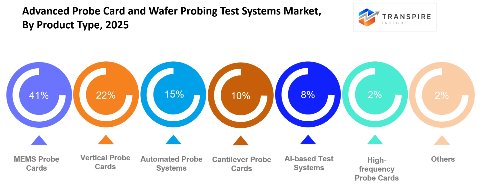
- MEMS Probe Cards have 41% of the market share as firms develop high-density probe cards to enhance test accuracy of advanced semiconductor nodes.
- Vertical Probe Cards constitute 22% of the market due to increased need for reliable testing of memory devices and semiconductor production.
- Automated Probe Systems are responsible for 15% market share, with firms adopting wafer handling automation to minimise testing time.
- Cantilever Probe Cards have a 10% market share and remain popular as an affordable testing option for mature semiconductor technologies.
- AI-Based Test Systems have 8% of the market and are the fastest-growing market segment with a CAGR of 20.5% thanks to predictive analytics and defect intelligence.
- High-frequency Probe Cards make up 2% of the market and are gaining popularity since radio frequency devices, 5G components and high-speed communication ICs require accurate signals.
- Specialised Probing Solutions account for 2% of the market and are used for testing niche semiconductor products, in research laboratories and in customised testing environments.
- Equipment makers in the semiconductor industry are enhancing their product portfolios through automation and artificial intelligence to minimise testing time and increase wafer yields.
What are the Key Drivers, Restraints, and Opportunities in the Advanced Probe Card and Wafer Probing Test Systems Market?
Drivers
The market is primarily characterised by the fast developments that are taking place in semiconductor technology and increasing production of efficient chips for applications such as artificial intelligence, electric cars, 5G technology, and other consumer electronics. Due to the reduction in size and increase in complexity of semiconductors, manufacturers require precise and accurate probe cards and wafer probing solutions in order to detect defects before the packaging process. The reduction in size of process nodes and integration density has compelled chip makers to utilise automated and precision testing solutions.
Restraints
One of the major barriers is the considerable amount of money needed to be invested in state-of-the-art probes and technologies and their regular upgrading. Advanced probe cards and AI testing stations are costly both to implement and operate. Also, compatibility problems with various sizes of wafers, chip structures, and production processes will increase operation expenses. For smaller semiconductor companies, such costs can be quite prohibitive due to limited budgets and low possibilities for implementation of more efficient solutions.
Opportunities
The opportunities are the establishment of advanced semiconductor fabrication facilities in Asia-Pacific, North America, and Europe, as well as growing interest in manufacturing with the use of artificial intelligence. Machine learning for predictive maintenance, real-time defect inspection, and automatic calibration opens up new areas for growth. Growing demand for advanced packaging, chiplet technology, and next-generation memory will only increase the demand for precise wafer probing and probe card solutions in the future.
What Has the Impact of Artificial Intelligence Been on the Advanced Probe Card and Wafer Probing Test Systems Market?
The use of artificial intelligence technology has led to an increase in performance efficiency of advanced probe card and wafer probing test systems due to increased speed, accuracy, and decreased dependence on manual inspection. With AI algorithms, huge amounts of data on wafers being tested can be analysed, and abnormalities and possible defects are detected to ensure that quality of production is not affected. As a result, semiconductor producers can achieve higher wafer yields, reduce errors in tests and reduce testing time at high-volume factories.
Predictive maintenance is another important application of AI. By monitoring equipment performance, AI can predict possible failures due to equipment wear or calibration problems. Thus, production downtime is reduced, maintenance costs are minimised and testing accuracy is ensured. Test optimisation using AI is another way of improving the process of testing through automatic adjustment of testing parameters depending on the device. Artificial intelligence implementation still has certain problems. The cost of implementation, complicated integration with the existing semiconductor manufacturing processes and the need for good-quality training data remain the main obstacles, especially for smaller companies. In May 2025, the Questa One intelligent verification platform from Siemens Digital Industries Software was announced, featuring the application of AI for automatic and predictive analysis to speed up IC verification and semiconductor testing productivity. The progress is relevant to the rising need for rapid and effective verification and testing processes of future AI-based chips alongside the rising use of advanced wafer probes and probe cards.
Key Market Trends:
The market is experiencing a significant transformation as semiconductor manufacturers utilise the latest testing technologies for smaller chip geometries, AI processors, and high-performance computing devices. Automated wafer probes, intelligence, and analytics are among the most important elements that allow semiconductor manufacturers to streamline production processes and keep the quality of products at a consistent level.
- Semiconductor testing techniques are gradually evolving from traditional manual testing to automation through highly automated wafer probing machines.
- MEMS probe cards have become more popular among chip manufacturers because they can provide higher levels of probing accuracy for advanced semiconductor nodes and complex architectures.
- There is a growing trend for semiconductor testing through AI-enabled platforms for data analysis, defect detection, and testing parameter optimization with minimum human interaction.
- High-frequency probe cards are gaining momentum thanks to the growth of 5G technology and radio frequency semiconductor devices.
- Semiconductor manufacturers are investing in smart manufacturing solutions that enable them to use digital monitoring for wafer probing machines and predictive maintenance.
- Custom testing solutions are being developed by probe card providers for chiplet technology, advanced packaging, and heterogeneous semiconductor integration.
Advanced Probe Card and Wafer Probing Test Systems MarketSegmentation
By Product Type
MEMS Probe Cards dominate the market by holding 41% market share due to their wide adoption in advanced semiconductor production due to better precision, reliability, and compatibility with finer pitch chips. Their capability to test high-density wafers has made them more popular and suitable for future semiconductor manufacturing needs. Vertical Probe Cards make up for 22% of the market since they are suitable for memory and logic device testing where stable electrical contact is necessary. Automated Probe Systems account for 15% of the market share due to the trend among semiconductor manufacturers to automate production facilities, increasing testing efficiency. Cantilever Probe Cards contribute 10% market share due to their use in mature semiconductors owing to their economical nature. AI-Based Test Systems make up 8% of the market and are estimated to record the highest CAGR of 20.5%. High-Frequency Probe Cards (2%) and Other (2%).
By Applications
The largest application area for semiconductors is that of fabrication, where wafer testing is becoming increasingly critical as an important quality check before packaging and assembling. Wafer testing is on the rise as more and more advanced processors, memory devices, and AI accelerators are being manufactured, which requires more accurate testing. IC packaging firms are employing advanced probing technologies for enhancing the reliability of packages, thereby reducing post-fabrication defects. An increasing demand is anticipated in the testing of memory devices, logic devices, RF components, and power semiconductors, backed up by rapid advancements in electric vehicles, industrial electronics, telecommunications, and computing applications.
By End User
Semiconductor foundries constitute the biggest end user segment as they need highly efficient wafer probing systems for maintaining the quality of production and increasing the yield of their production process. The OSAT companies are increasingly investing in automated probing systems for increasing their testing efficiency before packaging. The IDMs have a highly sophisticated probe card system for maintaining quality standards during production processes. The research centres are using the latest probing systems for creating new semiconductor materials and testing techniques, whereas the electronics industry depends on wafer probing systems for ensuring the performance of components in their consumer electronics, automotive electronics, industrial automation, and communication devices.
By Technology
MEMS technology is taking the lead since it helps achieve wafer contacts that are precise and reliable enough to be used in advanced semiconductor nodes. Vertical technology continues providing stability of the testing process for memories and mass production of chips. Automated tests enabled by AI technologies are developing rapidly as manufacturers adopt machine learning for automated defect detection, test parameter optimisation, and time reduction. High-speed automated tests are allowing semiconductor facilities to increase their efficiency and decrease manual efforts. Optical inspection is becoming more important as a way of detecting wafer defects before electrical testing, and hybrid probes are gaining importance in the era of new chip architecture and packaging technologies.
By Distribution Channels
The Direct Sale channel is predominant, since the semiconductor industry leaders usually purchase their customised testing equipment through the provider. The Semiconductor Equipment Distributors are becoming stronger in the market, as they distribute standard testing systems to the manufacturers in different regions. The OEM Suppliers are crucial, as they integrate new probe cards and wafer probing solutions into the overall semiconductor production line. The Exporters extend the international presence of testing equipment in the semiconductor centres, whereas others are specialised distribution partners that help small manufacturers and research organisations to procure customised testing solutions.
What are the Key Use Cases Driving the Advanced Probe Card and Wafer Probing Test Systems Market?
The advanced probe card and wafer probing test system market consists of various applications, and the major application area for this system is the semiconductor industry. In particular, the largest application type of this system in the semiconductor industry is the MEMS probe card that allows testing wafers before going into the packaging process. Other application areas for this technology beyond the traditional semiconductor industry include the testing of memory, RF devices, power semiconductors, and IC packaging. Increasing demands for automotive electronics, 5G network infrastructure, artificial intelligence hardware, and high-performance computing will drive the adoption of advanced wafer probing test systems. New emerging applications of this technology include the testing of chiplet architecture, advanced packaging, and future-generation AI accelerators.
|
Report Metrics |
Details |
|
Market size value in 2025 |
USD 3.2 Billion |
|
Market size value in 2026 |
USD 3.5 Billion |
|
Revenue forecast in 2033 |
USD 6.7 Billion |
|
Growth rate |
CAGR of 9.72% from 2026 to 2033 |
|
Base year |
2025 |
|
Historical data |
2021 - 2024 |
|
Forecast period |
2026 - 2033 |
|
Report coverage |
Revenue forecast, competitive landscape, growth factors, and trends |
|
Regional scope |
United States; Canada; Mexico; United Kingdom; Germany; France; Italy; Spain; Denmark; Sweden; Norway; China; Japan; India; Australia; South Korea; Thailand; Brazil; Argentina; South Africa; Saudi Arabia; United Arab Emirates |
|
Key company profiled |
FormFactor, Technoprobe, Micronics Japan, Tokyo Seimitsu, Advantest, MPI Corporation, Wentworth Laboratories, Feinmetall, SV Probe, Japan Electronic Materials, Cohu, TEL, Teradyne, MPI Technologies, Cascade Microtech. |
|
Customization scope |
Free report customization (country, regional & segment scope). Avail customized purchase options to meet your exact research needs. |
|
Report Segmentation |
By Product Type (Vertical Probe Cards, MEMS Probe Cards, Cantilever Probe Cards, Advanced Wafer Probers, Automated Probe Systems, AI-based Test Systems, High-frequency Probe Cards, Others); By Application (Semiconductor Manufacturing, Wafer Testing, IC Packaging, Memory Device Testing, Logic Device Testing, RF Device Testing, Power Semiconductor Testing, Others); By End User (Semiconductor Foundries, OSAT Companies, IDM Manufacturers, Research Institutes, Electronics Manufacturers, Test Laboratories, Others); By Technology (MEMS Technology, Vertical Technology, AI-enabled Testing, High-speed Automated Testing, Optical Inspection Integration, Hybrid Probe Technology, Others); By Distribution Channel (Direct Sales, Semiconductor Equipment Distributors, OEM Suppliers, Exporters, Others). |
Which Regions are Driving the Advanced Probe Card and Wafer Probing Test Systems Market Growth?
North America
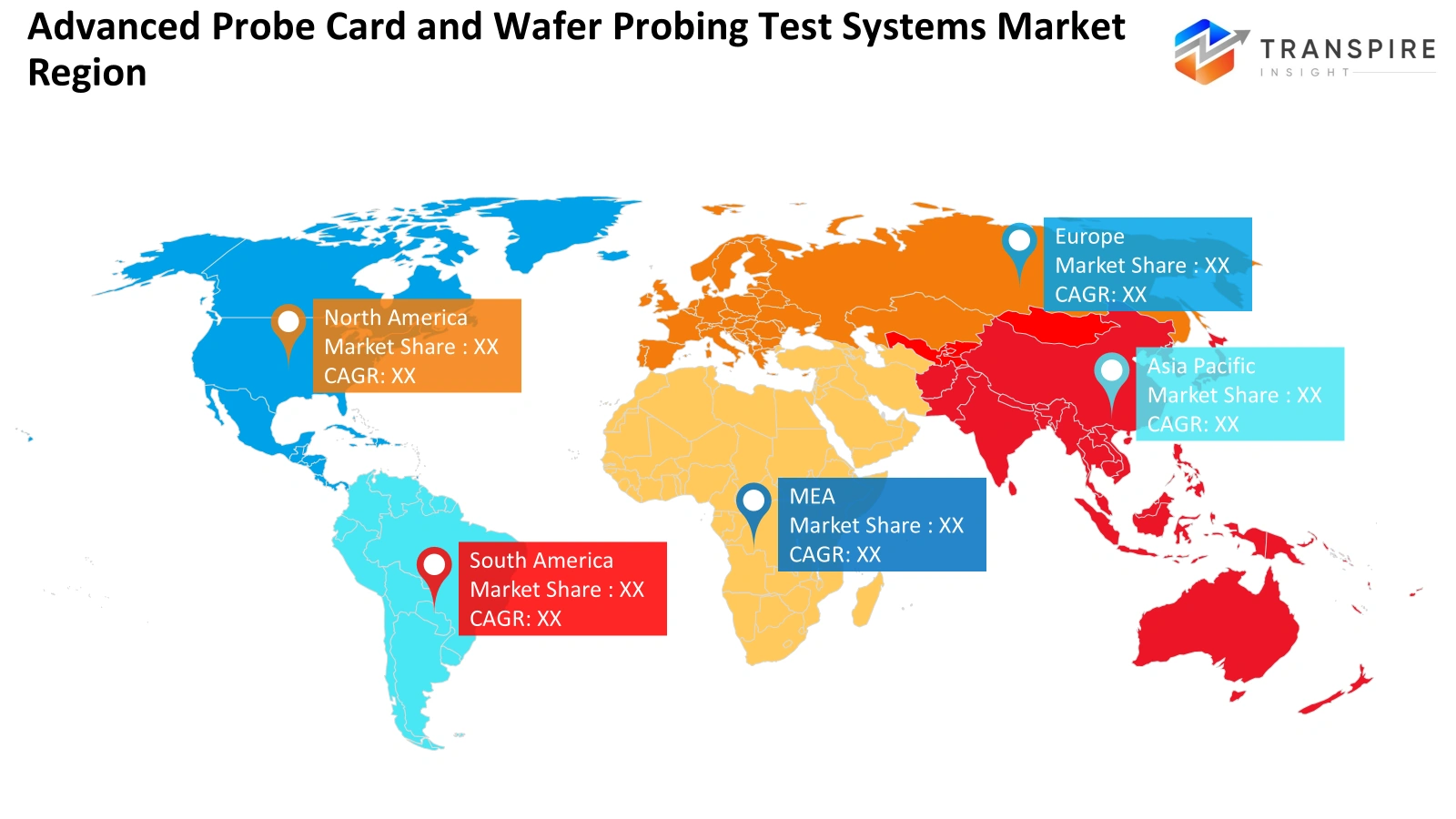
North America has a market share of 24%, which is the largest share, and the region is also expected to have the highest CAGR of 19.3%. The high investments made in semiconductor fabrication, AI processors, advanced computing, and future-generation semiconductor chip fabrication are the main drivers for growth in the region. Increased initiatives by governments for semiconductors, a high number of fabrication facilities, and growing demand for automated testing equipment are the factors contributing to market growth. All these are expected to provide enormous growth opportunities for advanced probe card and wafer probing technology manufacturers.
Europe
Europe accounts for a 23% share in the market and has been growing constantly due to its high involvement in the use of semiconductors in the automotive sector, industrial electronics and power semiconductors. Unlike the Asia Pacific region, Europe places importance on quality manufacturing, innovation and applications of semiconductors rather than mass manufacturing. Collaboration of research centres and semiconductor makers is driving the growth in wafer testing technology.
Asia-Pacific
The Asia-Pacific region is the leader in the Advanced Probe Card and Wafer Probing Test Systems Market, accounting for 47% of the market share owing to the robust semiconductor manufacturing landscape and investments in modern manufacturing plants. Countries like Taiwan, South Korea, China, and Japan have leading foundries and chip makers, leading to an increasing demand for precise wafer testing machines. The development of initiatives to bolster semiconductor production and capacity expansion activities further ensures the dominance of the region. The quick adoption of AI chips, advanced packaging solutions, and efficient processors is fuelling the demand for probe cards and automated wafer probing test systems.In February 2025, Advantest Corporation entered into a strategic alliance with Micronics Japan (MJC), which is one of the top probe card manufacturers in the world. This was done to improve the availability of advanced probe cards and offer high-performance semiconductor test solutions for AI, HPC and next-generation semiconductor devices.
Who are the Key Players in the Advanced Probe Card and Wafer Probing Test Systems Marketand how do they Compete?
The competitiveness in the worldwide Advanced Probe Card and Wafer Probing Test Systems market arises due to constant product innovations, sophisticated engineering, and strategic alliances with semiconductor producers. Due to the fact that the complexity of modern chip designs is growing, it is essential to enhance testing accuracy, automation processes, and compatibility with the smaller process nodes, along with increasing the capabilities of production and service provision on a scale.
Some of the most important players in the market include FormFactor Inc., Technoprobe S.p.A., MPI Corporation, Tokyo Seimitsu Co., Ltd. (Accretech), and Japan Electronic Materials Corporation (JEM). All of these organisations strive to develop innovative MEMS probe cards, highly efficient wafer probing test systems, and automated testing solutions. The large number of companies involved in the research and development process aims at providing custom solutions for memory devices, logic chips, artificial intelligence processors, and high-frequency semiconductors. Other companies such as Micronics Japan Co., Ltd. (MJC), FEINMETALL GmbH, Microfriend Inc., and SV Probe Pte. emphasise specific probe techniques, regional growth, and application-focused solutions. Collaboration, technological improvements, and enhanced support networks continue to be some of the competitive strategies as semiconductor production evolves into more advanced and automated production facilities.
Advanced Probe Card and Wafer Probing Test Systems Market companies
- FormFactor
- Technoprobe
- Micronics Japan
- Tokyo Seimitsu
- Advantest
- MPI Corporation
- Wentworth Laboratories
- Feinmetall
- SV Probe
- Japan Electronic Materials
- Cohu
- TEL
- Teradyne
- MPI Technologies
- Cascade Microtech
Recent Development News
In January 2025, Advantest Corporation made strategic partnerships and investment deals with Technoprobe S.p.A. and FormFactor Inc., where the two collaborated in order to develop next-generation probe cards, advance wafer-level testing solutions, and provide enhanced semiconductor testing solutions for AI and High Performance Computing devices.
Source: https://www.advantest.com
In March 2026, the MeasureOne partner program was extended by FormFactor Inc. and Rohde & Schwarz to offer turnkey RF test solutions. This involved integrating on-wafer probing technology with RF test instruments, which would enable semiconductor makers to achieve precise measurements with ease and minimise integration complications in product development.
Source: https://www.rohde-schwarz.com
What Strategic Insights Define the Future of the Advanced Probe Card and Wafer Probing Test Systems Market
The future of the Advanced Probe Card and Wafer Probing Test Systems Market is going to be driven by increasing investments made in semiconductor production technologies, artificial intelligence and increasingly intricate chip designs. As semiconductor producers start moving towards smaller process nodes and chiplets, the need for precision testing systems in wafer testing will only keep increasing. One thing that might not be known to everyone is that innovations in the semiconductor industry happen very rapidly, and it can actually shorten equipment lifecycles and force companies to update technologies frequently, thus increasing capital expenditures. On the other hand, new semiconductor fabrication facilities coming up in Asia Pacific, North America and Europe give great opportunities for suppliers of intelligent testing technologies. Companies that specialise in AI-driven analytics, MEMS probes and have close ties with the semiconductor foundry business will be able to increase their market share and position successfully.
Key Segmentations are:
By Product Type
- Vertical Probe Cards
- MEMS Probe Cards
- Cantilever Probe Cards
- Advanced Wafer Probers
- Automated Probe Systems
- AI-based Test Systems
- High-frequency Probe Card
By Application
- Semiconductor Manufacturing
- Wafer Testing
- IC Packaging
- Memory Device Testing
- Logic Device Testing
- RF Device Testing
- Power Semiconductor Testing
By End User
- Semiconductor Foundries
- OSAT Companies
- IDM Manufacturers
- Research Institutes
- Electronics Manufacturers
- Test Laboratories
By Technology
- MEMS Technology
- Vertical Technology
- AI-enabled Testing
- High-speed Automated Testing
- Optical Inspection Integration
- Hybrid Probe Technology
By Distribution Channel
- Direct Sales
- Semiconductor Equipment Distributors
- OEM Suppliers
- Exporters
Regional Outlook
North America
- United States
- Canada
- Mexico
Europe
- Germany
- United Kingdom
- France
- Spain
- Italy
- Rest of Europe
Asia Pacific
- Japan
- China
- Australia & New Zealand
- South Korea
- India
- Rest of Asia Pacific
South America
- Brazil
- Argentina
- Rest of South America
Middle East & Africa
- Saudi Arabia
- United Arab Emirates
- South Africa
- Rest of the Middle East & Africa
Frequently Asked Questions
Find quick answers to common questions.
The advanced probe card and wafer probing test systems market size was valued at USD 3.2 billion in 2025 and is poised to reach USD 6.7 billion by 2033, expanding at a 9.72% CAGR.
Key segments for the advanced probe card and wafer probing test systems market are By Product Type (Vertical Probe Cards, MEMS Probe Cards, Cantilever Probe Cards, Advanced Wafer Probers, Automated Probe Systems, AI-based Test Systems, High-frequency Probe Cards, Others); By Application (Semiconductor Manufacturing, Wafer Testing, IC Packaging, Memory Device Testing, Logic Device Testing, RF Device Testing, Power Semiconductor Testing, Others); By End User (Semiconductor Foundries, OSAT Companies, IDM Manufacturers, Research Institutes, Electronics Manufacturers, Test Laboratories, Others); By Technology (MEMS Technology, Vertical Technology, AI-enabled Testing, High-speed Automated Testing, Optical Inspection Integration, Hybrid Probe Technology, Others); By Distribution Channel (Direct Sales, Semiconductor Equipment Distributors, OEM Suppliers, Exporters, Others).
Growth is primarily driven by increased fabrication of semiconductors, high demand for AI, 5G, and automobile chips, developments in wafer testing technology, and increased investment in chip making.
The market is led by major manufacturers including FormFactor, Technoprobe, Micronics Japan, Tokyo Seimitsu, Advantest, MPI Corporation, Wentworth Laboratories, Feinmetall, SV Probe, Japan Electronic Materials, Cohu, TEL, Teradyne, MPI Technologies, Cascade Microtech.
The Asia Pacific region has a 47% share of the total market for probe cards & wafer probing test systems because of high semiconductor manufacturing capacity, high investment in chip fabrication, increased electronics manufacturing, and the presence of key foundry and testing companies in regions like Taiwan, South Korea, China, and Japan.
Commercial opportunities consist of higher demand for sophisticated semiconductor test equipment for chips used in artificial intelligence and high-performance computing, growth of the 5G and automotive electronics market, investment in new semiconductor wafer fab capacity, and use of MEMS and advanced packaging.
- FormFactor
- Technoprobe
- Micronics Japan
- Tokyo Seimitsu
- Advantest
- MPI Corporation
- Wentworth Laboratories
- Feinmetall
- SV Probe
- Japan Electronic Materials
- Cohu
- TEL
- Teradyne
- MPI Technologies
- Cascade Microtech
About the Authors

Avinash Kumar
I’m Avinash Kumar, a Senior Research Analyst at Transpire Insight, with expertise in the Electronics and Semiconductor and Energy & Power industry. My work focuses on analyzing emerging technologies, market trends, industry developments, and innovation across these sectors. I specialize in transforming complex technical and market insights into clear, research-backed content that helps professionals, businesses, and decision-makers stay informed. Through continuous industry research and data-driven analysis, I strive to deliver accurate, reliable, and practical perspectives on the latest advancements shaping the semiconductor and energy landscape.

Chakradhar Khansole
Chakradhar serves as the Research Director at Transpire Insight, bringing over 8 years of experience in technology, innovation, and strategic market intelligence. He specializes in transforming complex market data into actionable business insights that enable organizations to make informed, growth-oriented decisions. Recognized for his strategic vision and analytical expertise, Chakradhar leads high-impact research initiatives, delivering comprehensive market assessments, competitive intelligence, and forward-looking industry analysis.
Recently Published Reports
-
Apr 2026
Fiber Optic Faceplates Market
Fiber Optic Faceplates Market Size, Share & Analysis Report By Type (< 300 mm2, 300-350 mm2, and > 350 mm2, By Application (Night Vision, Holographic Imaging, Medical, and Others), and Geography (North America, Europe, Asia-Pacific, Middle East and Africa, South and Central America), 2021 - 2031
-
Apr 2026
High Temperature Superconductors Market
High Temperature Superconductors Market Size, Share & Analysis Report By Type (1G HTS, and 2G HTS), By Application (Power Cable, Fault Current Limiter, and Transformer), and Geography (North America, Europe, Asia-Pacific, Middle East and Africa, South and Central America), 2021 - 2031
-
Apr 2026
Industrial Plugs and Socket Market
Industrial Plugs and Socket Market Size, Share & Analysis Report By Type (Industrial Plugs, Industrial Sockets), By Current (Up to 32 A, 32 to 125 A, Above 125 A), By Protection (Dustproof and Splash Proof, Waterproof, Explosion Proof), By End User (Heavy Industries, Oil and Gas, Chemicals and Pharmaceuticals, Power Generation, Others), and Geography (North America, Europe, Asia-Pacific, Middle East and Africa, South and Central America), 2021 - 2031
-
Apr 2026
InGaAs Avalanche Photodiodes Market
InGaAs Avalanche Photodiodes Market Size, Share & Analysis Report By Type (1100 - 1700 nm, and 1000 - 1600 nm), By Application (Missile Warning System, Muzzle Flash Detection, Wafer Defect Inspection, Laser Rangefinders, and Others), and Geography (North America, Europe, Asia-Pacific, Middle East and Africa, South and Central America), 2021 - 2031