
Aug 17, 2026
By Transpire Insight
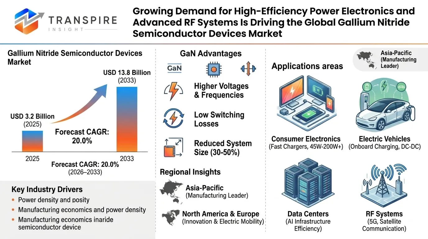
The Gallium Nitride Semiconductor Devices Market is undergoing rapid technological expansion as industries increasingly require semiconductor components capable of operating at higher voltages, frequencies, temperatures, and power densities than conventional silicon devices can efficiently support. Gallium nitride (GaN) is a wide-bandgap semiconductor material with a bandgap of approximately 3.4 eV, substantially higher than silicon at around 1.1 eV. This fundamental material advantage allows GaN devices to operate with lower switching losses, higher breakdown voltages, and greater thermal and electrical efficiency, making them increasingly important across power electronics, radio-frequency communication, automotive systems, consumer electronics, aerospace, defense, and renewable-energy applications.
According to Transpire Insights, the Gallium Nitride Semiconductor Devices Market was valued at approximately USD 3.2 billion in 2025 and is expected to reach around USD 13.8 billion by 2033, representing a forecast CAGR of approximately 20.0% during 2026–2033. The market is transitioning from an early-adoption technology toward broader commercial deployment as manufacturers improve wafer production, device reliability, packaging technologies, and manufacturing economics. Increasing demand for compact power supplies, fast chargers, electric vehicles, 5G infrastructure, satellite communication, and high-efficiency energy systems is creating multiple avenues for GaN device adoption.
The fundamental attraction of GaN technology comes from its ability to deliver higher power density while reducing energy losses. In suitable applications, GaN power devices can achieve switching frequencies several times higher than traditional silicon-based components, allowing engineers to reduce the size of inductors, transformers, capacitors, and other passive components. This can result in power systems that are approximately 30–50% smaller and lighter than comparable conventional designs, depending on application requirements and circuit architecture. The resulting reduction in system size is particularly valuable for consumer electronics, electric mobility, aerospace equipment, and data-center power infrastructure, where space and weight have a direct economic impact.
The consumer electronics industry has become one of the most visible commercial applications of GaN semiconductor devices. GaN-based chargers can operate at higher switching frequencies and deliver substantial power from relatively compact form factors. Chargers in the 45 W, 65 W, 100 W, 140 W, and above 200 W categories are increasingly incorporating GaN technology, particularly for smartphones, tablets, laptops, gaming systems, and other portable electronics. The ability to replace larger silicon-based power components with smaller GaN systems has created strong demand from manufacturers seeking thinner devices and more energy-efficient charging products.
The growth of fast-charging infrastructure is expected to provide another important source of demand. Modern consumers increasingly expect smartphones, computers, and other portable devices to achieve substantial battery replenishment within 15–60 minutes, depending on battery capacity and charging architecture. GaN devices support high-frequency switching and efficient power conversion, allowing charger manufacturers to deliver higher power ratings without proportionally increasing physical dimensions. As fast charging becomes a standard feature across consumer electronics, GaN adoption is expected to expand beyond premium products into increasingly mainstream devices.
The transition toward electric vehicles is creating a much larger long-term opportunity for GaN technology. Electric vehicles require highly efficient power-conversion systems for onboard charging, DC-DC conversion, battery management, auxiliary power systems, and increasingly sophisticated electronic architectures. While silicon carbide currently has a stronger position in several high-voltage traction applications, GaN is particularly attractive for lower- and medium-voltage power-conversion applications where high switching frequency, compactness, and efficiency provide significant advantages.
The automotive electronics environment is becoming substantially more demanding as vehicle manufacturers introduce advanced driver-assistance systems, infotainment, connected features, electronic control units, wireless charging, and increasingly software-defined vehicle architectures. Modern vehicles can contain hundreds of semiconductor-based electronic control functions, creating opportunities for GaN components in power-management systems and high-frequency applications. As vehicle electrical architectures move toward higher voltage levels, including 400 V and 800 V platforms, semiconductor efficiency becomes increasingly important for minimizing energy losses.
Data centers represent another strategically important market. The rapid expansion of cloud computing, artificial intelligence, machine learning, and high-performance computing is increasing electricity consumption and creating significant pressure to improve power-conversion efficiency. In large data centers, even a 1% improvement in power-conversion efficiency can translate into meaningful reductions in electricity consumption, cooling requirements, and operating costs because facilities may consume electricity at the scale of tens to hundreds of megawatts.
Regional development is also becoming increasingly significant. Asia-Pacific is expected to remain the leading regional market because of its extensive semiconductor manufacturing ecosystem, consumer electronics production, telecommunications infrastructure, electric-vehicle manufacturing, and rapidly expanding renewable-energy capacity. China, Japan, South Korea, and Taiwan are particularly important to the GaN supply chain, while India is emerging as an increasingly relevant electronics and semiconductor manufacturing market.
North America is expected to maintain strong demand because of advanced data centers, defense programs, aerospace applications, electric vehicles, and semiconductor technology development. The region is also home to several important GaN technology companies and research institutions, supporting continued innovation in power and RF devices.
Europe is developing significant opportunities through electric mobility, renewable energy, industrial automation, aerospace, and high-efficiency power systems. European automotive manufacturers and industrial technology companies are increasingly focused on improving power-conversion efficiency and reducing system weight, creating opportunities for wide-bandgap semiconductor technologies.
Download the exclusive Gallium Nitride Semiconductor Devices Market sample report today to uncover expert insights, emerging trends, and the opportunities defining the future of the industry.
Expanding Power Electronics, Fast-Charging Infrastructure, Data Centers, and RF Communication Systems Are Accelerating GaN Semiconductor Adoption
The Global Gallium Nitride Semiconductor Devices Market is increasingly benefiting from the transition toward high-efficiency power conversion and high-frequency electronic systems. According to Transpire Insights, the primary structural change supporting GaN adoption is the growing requirement to achieve greater electrical performance from smaller and lighter electronic architectures. Conventional silicon devices remain widely used because of their established manufacturing infrastructure and comparatively low cost, but their performance becomes increasingly constrained as switching frequencies, power densities, and efficiency requirements rise. GaN addresses several of these limitations by enabling faster switching and lower losses, making it particularly suitable for applications where every watt of saved energy and every cubic centimeter of reduced system volume can have commercial value.
The power electronics segment represents one of the most important demand centers for GaN semiconductor devices. Power supplies, adapters, converters, inverters, and charging systems increasingly require switching frequencies that can reach several hundred kilohertz or even into the megahertz range. GaN devices can operate at substantially higher frequencies than many conventional silicon power components, allowing designers to reduce the size of magnetic components and other passive elements. In suitable architectures, this can contribute to system-volume reductions of approximately 30–50%, while improving power density and reducing cooling requirements.
Consumer charging equipment has become the most visible commercialization pathway for GaN technology. The expansion of USB-C and increasingly powerful charging standards has encouraged manufacturers to introduce compact chargers capable of supporting multiple devices simultaneously. Chargers in the 65–140 W range have become increasingly common in laptops and premium consumer electronics, while higher-power products exceeding 200 W are also entering specialized markets. The ability to deliver these power levels through compact adapters has helped establish GaN as a practical alternative to conventional silicon-based power solutions.
The commercial importance of fast charging extends beyond smartphones and laptops. Portable gaming systems, professional workstations, monitors, smart-home equipment, industrial handheld devices, and electric mobility accessories increasingly require higher power from smaller adapters. As consumers become accustomed to faster charging and manufacturers attempt to reduce electronic product dimensions, GaN's power-density advantage becomes increasingly relevant. The growing adoption of multi-port charging systems is also creating opportunities because one GaN-based power supply can dynamically distribute 100 W, 140 W, 200 W, or more across several connected devices.
Another major development is the increasing integration of GaN devices into power-factor correction and power-management systems. Modern electronic equipment must efficiently convert electricity from the grid into usable DC power while minimizing losses. GaN's high switching speed allows designers to optimize these conversion stages using smaller passive components and advanced circuit topologies. In high-utilization equipment, even relatively small improvements in conversion efficiency can generate significant lifetime energy savings.
Data centers are therefore emerging as a particularly important long-term opportunity. The rapid growth of artificial intelligence and high-performance computing is increasing the amount of electricity consumed by servers, accelerators, networking equipment, and cooling systems. Modern AI-oriented data-center racks can require power levels of 30–100 kW or more per rack, with some next-generation architectures expected to exceed these levels. At such power densities, improving the efficiency of each conversion stage becomes increasingly important.
GaN devices can contribute to this transformation through server power supplies, intermediate bus converters, power-factor correction systems, and other power-management architectures. If a large facility improves power-conversion efficiency by even 1–2 percentage points, the resulting reduction in energy losses can become substantial when multiplied across thousands of servers operating continuously. Lower losses also reduce heat generation, which can decrease the amount of energy required for cooling and improve overall data-center efficiency.
The development of 800 V-class data-center power architectures is expected to create additional opportunities for advanced semiconductor technologies. As AI processors demand increasingly large amounts of electricity, data-center operators are exploring higher-voltage distribution architectures to reduce current levels and improve power-delivery efficiency. GaN can participate in selected high-frequency conversion stages within these systems, particularly where high switching performance and compact power conversion are required.
Electric vehicles represent another important area of development, although the competitive environment differs from consumer electronics. Silicon carbide has established a strong position in high-voltage traction inverters, while GaN is increasingly being evaluated for auxiliary power conversion, onboard charging, DC-DC conversion, battery-related systems, and other applications where high-frequency switching provides a distinct advantage. Automotive designers are increasingly focused on reducing the size and weight of power electronics because vehicle efficiency is influenced not only by battery capacity but also by the mass and electrical losses of supporting systems.
Semiconductor Manufacturing Advances, Wafer Scaling, AI Infrastructure, and High-Frequency Applications Are Expanding the Global Gallium Nitride Semiconductor Devices Market
The Global Gallium Nitride Semiconductor Devices Market is moving into a more mature phase as improvements in semiconductor manufacturing, device architecture, packaging, and system integration gradually expand GaN beyond its initial applications in premium chargers and radio-frequency equipment. According to Transpire Insights, the technology is increasingly being evaluated according to its total system-level value rather than simply its transistor-level performance. This distinction is important because GaN can justify its higher component cost when its higher switching frequency, reduced losses, smaller passive components, lower thermal requirements, and greater power density produce measurable savings across the complete electronic system.
One of the most important developments influencing the market is the continuing improvement in GaN wafer manufacturing. Semiconductor producers are increasingly working with larger wafer formats, improved epitaxial layers, higher manufacturing yields, and better defect-control techniques. The movement from smaller wafer platforms toward 6-inch and 8-inch wafers is particularly important because larger wafers allow manufacturers to produce a greater number of semiconductor dies during each manufacturing cycle. If yield improvements occur simultaneously, the cost per device can decline substantially, making GaN more competitive in applications where silicon remains dominant because of its established low-cost manufacturing ecosystem.
Proceed to Checkout to purchase the exclusive Gallium Nitride Semiconductor Devices Market report and gain instant access to in-depth market intelligence, strategic analysis, and future growth opportunities.
The economics of GaN manufacturing are closely connected to yield. A semiconductor wafer may contain hundreds or thousands of individual devices depending on die dimensions, while only a portion of the wafer can ultimately become saleable products after processing and testing. Even a 5–10 percentage-point improvement in manufacturing yield can have a meaningful impact on production economics when multiplied across large-scale manufacturing volumes. Consequently, semiconductor companies are investing heavily in process control, epitaxial growth, defect reduction, wafer inspection, and automated testing.
The underlying material characteristics of GaN continue to provide the foundation for this investment. With a bandgap of approximately 3.4 eV, GaN can tolerate stronger electric fields than silicon and can operate effectively under demanding high-frequency conditions. GaN's high electron mobility and high breakdown field make it particularly suitable for applications requiring rapid switching. In power electronics, this enables designers to increase switching frequency from conventional ranges of hundreds of kilohertz toward 1 MHz and beyond in selected architectures. Higher switching frequency reduces the physical size of magnetic components, although actual system performance depends heavily on circuit design, thermal management, and packaging.
This higher-frequency capability is particularly valuable in compact power supplies. Traditional power converters often require relatively large transformers, inductors, capacitors, and heat sinks because of switching-frequency limitations. Increasing the operating frequency allows these components to become smaller. As a result, GaN-based power systems can potentially achieve power densities several times higher than older silicon-based designs. In compact consumer chargers, for example, a higher-power GaN adapter can occupy substantially less volume than an equivalent conventional charger while delivering similar or greater output power.
The transition toward USB-C Power Delivery is strengthening this opportunity. Modern USB-C systems can support power levels ranging from relatively low charging requirements to more than 200 W in advanced implementations. This broad power range is encouraging manufacturers to develop chargers capable of powering smartphones, tablets, laptops, monitors, and other devices through a single compact adapter. GaN is particularly suited to these designs because manufacturers can use high switching frequencies to reduce component dimensions without sacrificing the required power output.
The technology is also becoming increasingly relevant to AI infrastructure. The rapid development of artificial intelligence has increased demand for graphics processors, AI accelerators, high-bandwidth memory, networking equipment, and high-performance computing systems. These components consume substantial amounts of electricity and require highly efficient power delivery. Modern AI data-center racks can operate at power levels of 30–100 kW or more, creating significant engineering pressure to improve power conversion at every stage.
As rack power density increases, conventional low-voltage distribution architectures become increasingly difficult to optimize because higher current levels require larger conductors and create greater resistive losses. The industry is therefore exploring higher-voltage power-distribution architectures, including systems operating around 400–800 V DC within data-center environments. GaN can participate in several conversion stages within these architectures, particularly where high-frequency switching and compact power conversion are required.
Competitive Landscape, Regional Expansion, Investment Strategies, and Commercialization Trends in the Global Gallium Nitride Semiconductor Devices Market
The competitive structure of the Global Gallium Nitride Semiconductor Devices Market is becoming increasingly diversified as semiconductor manufacturers, power-electronics companies, RF technology providers, and vertically integrated electronics manufacturers expand their participation in GaN technology. According to Transpire Insights, the market is gradually moving from a relatively concentrated technology-development stage toward a broader commercialization phase in which manufacturing scale, device reliability, application-specific engineering, packaging capabilities, and customer relationships are becoming as important as the underlying semiconductor technology. Companies are therefore competing not only on transistor performance but also on the ability to deliver complete solutions that can be integrated into chargers, data-center power supplies, telecommunications equipment, automotive systems, and advanced RF platforms.
Major participants associated with the GaN ecosystem include Infineon Technologies AG, Wolfspeed, Inc., Qorvo, Inc., Nexperia, Navitas Semiconductor, Inc., ROHM Co., Ltd., Mitsubishi Electric Corporation, Panasonic Holdings Corporation, Texas Instruments Incorporated, and Transphorm, Inc., together with several specialized and emerging semiconductor companies. These organizations have different areas of concentration. Some focus primarily on GaN power devices, while others have stronger positions in RF applications, integrated power systems, semiconductor manufacturing, or industrial electronics. This specialization is creating a competitive environment in which application expertise increasingly determines commercial success.
Infineon Technologies AG has a broad position across power semiconductors and automotive electronics, allowing it to integrate GaN technology into a wider portfolio of power-management products. The company's scale in industrial and automotive semiconductor markets provides access to customers already familiar with wide-bandgap technologies. This creates an opportunity to position GaN alongside silicon and silicon carbide rather than treating the technologies as direct substitutes. In practice, customers can select the semiconductor technology according to voltage, switching frequency, efficiency, thermal requirements, and cost.
Navitas Semiconductor has developed a particularly strong association with GaN power ICs and fast-charging applications. Its strategy illustrates the growing importance of integrating the GaN transistor with gate-drive and control functions. Integration can reduce external component requirements and simplify system design. In certain applications, integrated GaN power systems can reduce component counts by approximately 20–40%, while also improving switching performance and reducing parasitic losses.
The RF market has a different competitive structure, with companies such as Qorvo and other RF semiconductor specialists targeting telecommunications, aerospace, defense, radar, and satellite communication applications. GaN RF devices can operate at high frequencies while delivering substantial output power, making them attractive for applications where traditional silicon-based RF technologies face performance limitations. The RF segment is particularly important because defense and aerospace customers may purchase relatively lower unit volumes but require technically sophisticated devices with higher average selling values and long qualification cycles.
The competitive environment is also being influenced by vertical integration. Semiconductor companies are increasingly seeking greater control over epitaxial materials, wafer processing, device fabrication, packaging, and testing. Vertical integration can improve supply-chain reliability and provide greater control over manufacturing yields. This becomes strategically important because GaN manufacturing requires specialized process expertise, and disruptions in epitaxial wafer or semiconductor fabrication capacity can affect downstream device availability.
Investment in manufacturing capacity is therefore becoming a major competitive differentiator. Establishing or upgrading a GaN manufacturing facility can require investments ranging from tens of millions to several hundred million dollars, depending on the scale and whether the facility uses dedicated or converted semiconductor production infrastructure. Companies that can achieve high factory utilization and stable production yields are likely to have an advantage because semiconductor manufacturing economics depend strongly on fixed-cost absorption.
Schedule a meeting with our market experts to discuss the exclusive Gallium Nitride Semiconductor Devices Market report and identify the best research solution for your organization.
Conclusion
The market's future growth will be supported by the rapid adoption of fast-charging systems, AI data centers, electric vehicles, 5G and future 6G infrastructure, renewable-energy systems, satellite communications, aerospace, defense, and industrial automation. GaN's ability to operate at switching frequencies of 1 MHz and beyond in suitable architectures can enable smaller magnetic components, while system-level efficiency improvements of approximately 2–5% can create substantial energy savings in high-utilization applications. Similarly, reductions of 20–40% in selected component counts through integrated GaN solutions can improve product size, reliability, and manufacturing efficiency.
Technological improvements in 6-inch and 8-inch wafer manufacturing, epitaxial growth, packaging, thermal management, and integrated power architectures are expected to progressively reduce production costs and strengthen commercial adoption. Although silicon and silicon carbide will continue to serve important application areas, GaN is establishing a distinct position where high-frequency operation, compactness, efficiency, and RF performance are critical. As manufacturing scale increases and automotive and industrial qualification improves, the technology is expected to penetrate increasingly demanding applications.
Overall, the Global Gallium Nitride Semiconductor Devices Market is expected to evolve into an important pillar of next-generation power electronics and RF systems. The convergence of energy-efficiency requirements, electronic miniaturization, artificial intelligence, electrification, renewable energy, and advanced communications will continue creating opportunities for semiconductor manufacturers and technology providers through 2033 and beyond.


Send us a brief description of your challenge and we'll get back to you within 24 hours.

 inquiry@transpireinsight.com
 APAC:+91 7666513636
 Address


