
Wafer Fabrication Equipment Market Summary:
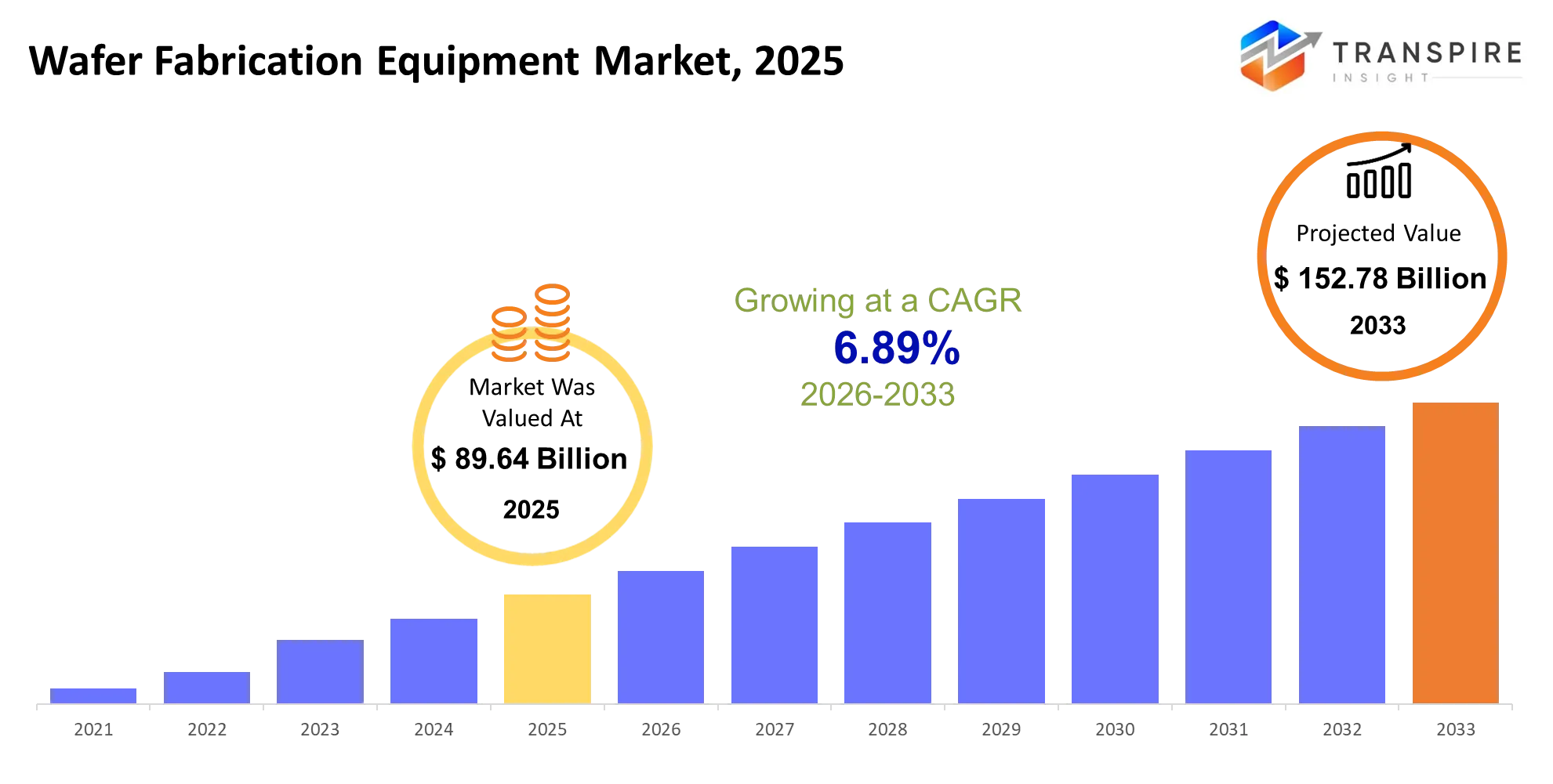
As per Transpire Insight, the Wafer Fabrication Equipment Market size is estimated at USD 89.64 billion in 2025 and is anticipated to reach USD 152.78 billion by 2033, growing at a CAGR of 6.89% from 2026 to 2033.
The wafer fabrication equipment market provides the machines that are used to pattern, deposit, remove, clean, modify, measure and inspect semiconductor wafers before the chips go into packaging. In the past three to five years, spending has moved toward advanced logic, high-bandwidth memory, advanced packaging and more complicated process nodes. A major change is the move toward smaller sizes and three-dimensional chip structures, which means more precise process control and better equipment is needed. The real reason behind this is the growth of AI computing infrastructure, which has made chipmakers want to increase leading-edge and memory capacity. With increased need for AI and the data centre industry, there will be an increase in investment in semiconductors, which in turn will cause increased investments in the factories that will make increased investments in equipment purchases, and upgrading to the latest technology will add value to every process involved.
Wafer Fabrication Equipment Market Size & Forecast:
- Market Size 2025: USD 89.64 Billion
- Expected Market Value (2033): USD 152.78 Billion
- Forecast CAGR (2026–2033): 6.89%
- Leading Region in 2025: Asia Pacific
- Fastest Growing Region: North America
- Key Company Profiles: ASML, Applied Materials, Lam Research, Tokyo Electron, KLA Corporation, ASM International, SCREEN Holdings, Hitachi High-Tech, Canon, Nikon, Teradyne, Onto Innovation, Axcelis Technologies, ASMPT, Disco Corporation
Key Market Insights:
The market is shifting toward technology complexities at advanced nodes, AI infrastructure, and equipment intelligence, as opposed to pure capacity expansion.
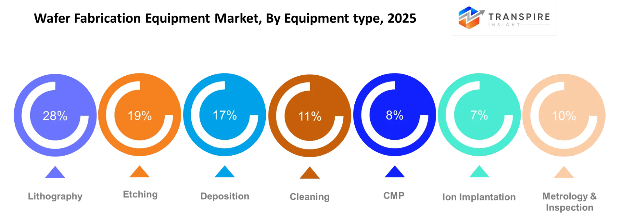
- Lithography equipment accounts for 27.80% of total market value, making it the largest in terms of pattern capability.
- ASML is leveraging lithography technology from scanner equipment to computational lithography, metrology, inspection, and AI-driven optimisation.
- Advanced lithography technology leads growth with a CAGR of 9.80%, driven by the increased patterning requirements for new nodes.
- Etch holds 19.00%, due to increased complexity of devices necessitating selective and controlled material removal.
- Deposition accounts for 17.00%, due to increase in the requirement of atomic-scale and three-dimensional structures.
What are the Key Drivers, Restraints, and Opportunities in the Wafer Fabrication Equipment Market?
Drivers:
The increase in the market is the demand for advanced nodes, and each node needs better control on patterning, deposition, etching, cleaning, and inspection processes. AI Computing has been responsible for this transition because of its investments in the development of future-generation logic, DRAM, and advanced packaging. As a result of the reduction in chip geometry and 3D structures, the industry will require equipment to enhance precision, yield, productivity, and process repeatability.
Restraints:
The limitation to market growth is the expensive nature of the advanced fabrication equipment. Advanced equipment will demand complex optics, vacuum technology, sensors, software, materials science, and expertise. This will make it difficult to qualify the systems and lead to delays in equipment purchases, particularly for greenfield factories. Concentration in the supply chain of components will keep this limitation structural and not cyclical.
Opportunities:
Opportunities involve the development of manufacturing operations for next-generation nodes and AI applications in new geographic locations. The construction of a fab and other manufacturing infrastructure such as 300 mm fabrication and advanced packaging generates opportunities to create equipment ecosystems. For instance, ASML’s investment in Tata Electronics is meant to ensure the creation of a 300 mm fab in Dholera, India. On the other hand, Applied Materials is growing its manufacturing capacity in Singapore to manufacture semiconductors using AI.
What Has the Impact of artificial intelligence on the Wafer Fabrication Equipment Market?
The use of AI is becoming integral to the fabrication equipment itself rather than just a source of demand for the chips. The equipment providers are employing machine learning, sensing, digital twins, and feedback loops in order to achieve better control of the processes, identify the defects, optimise recipes, and reduce unplanned downtime. ASML has stated that the use of AI is integral to computational lithography, metrology, and inspection, where it can help with optical proximity correction, defect detection, inspection sampling, and prediction of heating impact on the reticles. Lam Research is also implementing sensing, data, algorithms, AI, and automation through its Equipment Intelligence offerings.
The adoption is facing some constraints such as high costs of integration with the old tools, good-quality process data, the need for model validation, cybersecurity needs, and the risk of wrong prediction due to changed manufacturing conditions. The market impact, thus, is most pronounced in the case of AI integration with sensors and process-control systems.
Instance:
In June 2026, Applied Materials unveiled new semiconductor production systems aimed at DRAM and advanced packaging in AI chips. Technologies covered by this announcement were deposition, chemical mechanical planarization, epitaxy and e-beam metrology, showing how rising demands of artificial intelligence have boosted investments in wafer production equipment.
Key Market Trends:
Market trends towards equipment requirements will progress to a more integrated and automated stage since chip designs will get more complicated.
- transistors have been evolving towards GAA transistors and 3D architectures, thus requiring advanced etching and deposition technologies.
- Since the advent of generative AI, semiconductor manufacturers have been making increased investments in advanced production capabilities in logic and HBM. SEMI
- 300 mm wafer fabrication continues to influence the market due to the productivity associated with larger diameter wafers and is crucial in advanced volume manufacturing.
- AI and machine learning are increasingly entering the production equipment world, providing functions such as defect classification, recipe optimisation, predictive control, and predictive maintenance.
- Semiconductor strategies have been influenced by regional semiconductor plans to build fabs outside the traditional areas, which increases local equipment support demand.
Wafer Fabrication Equipment Market Segmentation
By Type of Equipment:
lithography equipment holds the biggest share of 27.80%, followed by etching with 19.00% and deposition with 17.00%. 11.00% goes to cleaning, 8.00% to CMP, 7.00% to ion implantation, 6.00% to metrology and inspection, and 4.20% to other types of equipment, the sum being 100%. Lithography dominates because pattern accuracy is critical in manufacturing advanced-node chips, while etch and deposition play a larger role as structures get more complicated and deeper. Advanced lithography is the market’s most dynamically developing sector with 9.80% CAGR, which suggests that future demand for equipment will be more about precision and better process control.
By Wafer Size:
the industry includes 100 mm, 150 mm, 200 mm, 300 mm, and 450 mm wafer platforms, as well as speciality and advanced wafers. Large wafer platforms, especially the 300 mm one, still have significance for high-volume manufacturing due to providing a larger number of devices per production run. Small wafers will also have their role in mature, speciality, power, MEMS and research wafer segments.
By Process:
The equipment needs are for front-end processing, back-end processing, wafer cleaning, wafer inspection, patterning, deposition and etching. The front-end processes continue to be associated with logic and memory scaling, whereas the back-end processes are becoming important because of the increasing complexity of packaging. There is an increased need for precise control in the case of patterning, deposition and etching processes due to reduction in size and three-dimensional device structures. Integration of processes is the key future opportunity for equipment suppliers.
By Technology Node:
the market segments are above 180nm, 130-180nm, 90-130nm, 45-90nm, 22-45nm, 7-22nm and below 7nm processes. The mature nodes continue to be used in automotive, industrial, power, analogue, and other applications, while small nodes would require patterning, deposition, etching, metrology and inspection to be highly advanced. There is growth at a CAGR of 9.80% in advanced lithography due to the increased equipment intensity due to smaller geometries.
By Application:
The wafer fabrication equipment is used for making memory, logic, foundry, analogue, power semiconductor, MEMS, imaging sensors, and RF devices. Logic and foundry have a strong correlation to high-performance computing and leading-edge node spending, while memory spending is linked to the requirements from data centres and AI. Applications like power, analogue, MEMS, imaging sensors, and RF devices make an end market that is diverse in nature and hence does not depend on only one semiconductor application.
By End User:
The market includes integrated device manufacturers, foundries, memory manufacturers, fabless companies, research institutions, OSATs, and government labs. The major end users that buy equipment are still IDMs, foundries, and memory manufacturers because they have fabrication plants. However, research institutions and government labs play an important role in developing new technologies and processes. The OSAT market is becoming increasingly relevant due to advances in advanced packaging, thus creating demand for inspection, deposition, CMP, and other processes.
What are the Key Use Cases Driving the Wafer Fabrication Equipment Market?
The lithography technique is a use case since the fabrication of wafers is carried out through lithography technology. This is due to the fact that lithography technologies account for the biggest part of the industry and therefore depend on the logic, memory, and foundry process demand that have yield and performance considerations depending on the accuracy of the pattern. Etch, deposition, clean, CMP, ion implantation, and metrology are combined to create multi-layer structures. The systems are used in memory, logic, analogue, power semiconductors, MEMS, image sensors, and RF device manufacturing, where advanced packaging creates increased requirements for inspections. The new use cases are artificial intelligence accelerators, high-bandwidth memory, three-dimensional structures, and advanced packaging. Digital twins, machine learning, and automatic inspection are aiding in process development and minimising wafer run requirements.
|
Report Metrics |
Details |
|
Market size value in 2025 |
USD 89.64 Billion |
|
Market size value in 2026 |
USD 95.83 Billion |
|
Revenue forecast in 2033 |
USD 152.78 Billion |
|
Growth rate |
CAGR of 6.89% from 2026 to 2033 |
|
Base year |
2025 |
|
Historical data |
2021 - 2024 |
|
Forecast period |
2026 - 2033 |
|
Report coverage |
Revenue forecast, competitive landscape, growth factors, and trends |
|
Regional scope |
United States; Canada; Mexico; United Kingdom; Germany; France; Italy; Spain; Denmark; Sweden; Norway; China; Japan; India; Australia; South Korea; Thailand; Brazil; Argentina; South Africa; Saudi Arabia; United Arab Emirates |
|
Key company profiled |
ASML, Applied Materials, Lam Research, Tokyo Electron, KLA Corporation, ASM International, SCREEN Holdings, Hitachi High-Tech, Canon, Nikon, Teradyne, Onto Innovation, Axcelis Technologies, ASMPT, Disco Corporation |
|
Customization scope |
Free report customization (country, regional & segment scope). Avail customized purchase options to meet your exact research needs. |
|
Report Segmentation |
Equipment Type (Lithography Equipment, Etching Equipment, Deposition Equipment, Cleaning Equipment, CMP Equipment, Ion Implantation Equipment, Metrology & Inspection, Wafer Processing Equipment); Wafer Size (100 mm, 150 mm, 200 mm, 300 mm, 450 mm, Specialty Wafers, Advanced Wafers); Process (Front-End Processing, Back-End Processing, Wafer Cleaning, Wafer Inspection, Patterning, Deposition, Etching); Technology Node (Above 180 nm, 130–180 nm, 90–130 nm, 45–90 nm, 22–45 nm, 7–22 nm, Below 7 nm); Application (Memory, Logic, Foundry, Analog, Power Semiconductor, MEMS, Image Sensors, RF Devices); End User (IDMs, Foundries, Memory Manufacturers, Fabless Companies, Research Institutes, OSATs, Government Labs) |
Which Regions are Driving the Wafer Fabrication Equipment Market Growth?
North America:
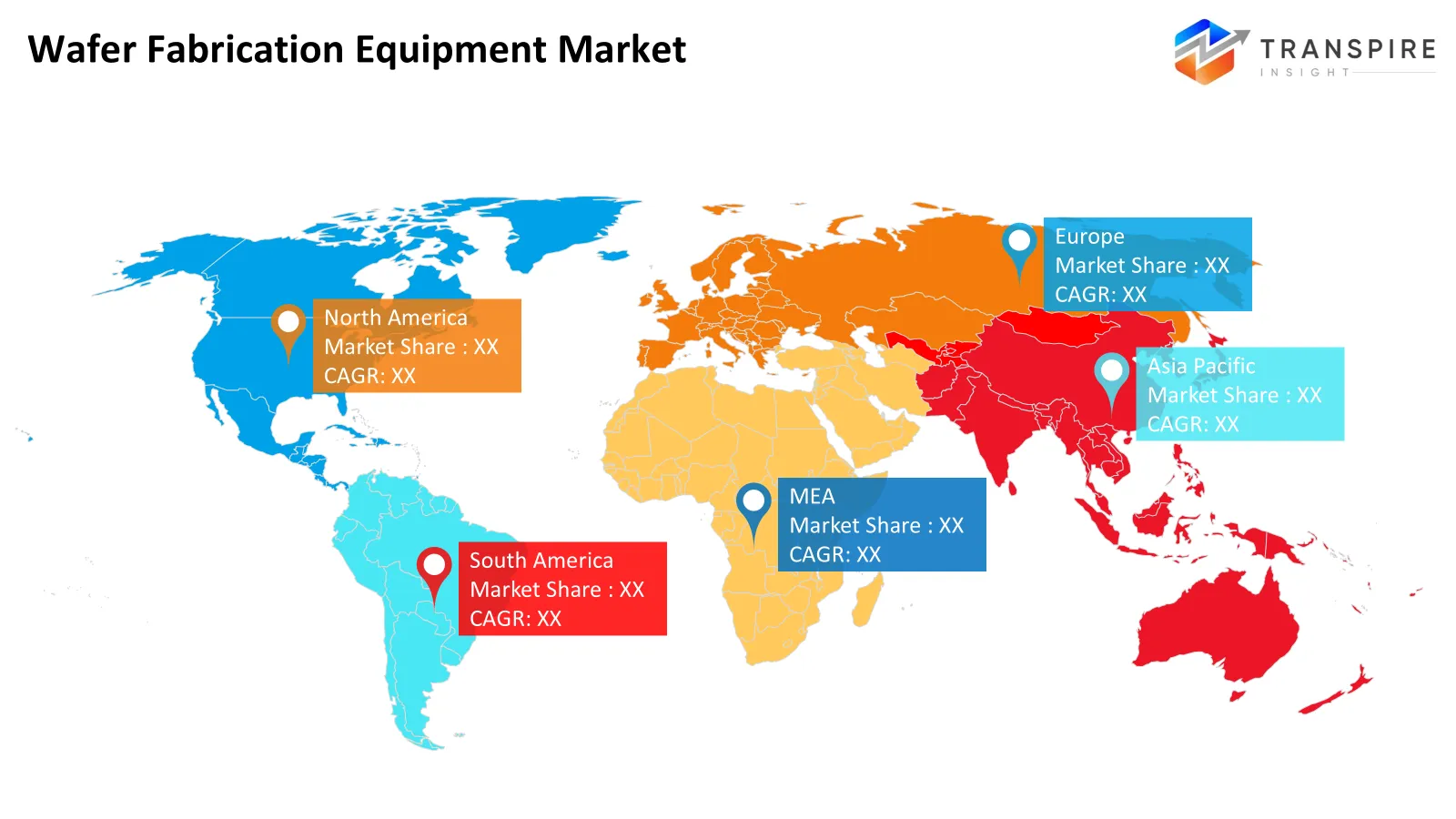
North America accounts for 17.00% market share and is the fastest-growing region with a forecast CAGR of 7.20%. It is driven by increased semiconductor investments domestically, logic development, infrastructure for AI, and attempts to reinforce chip supply chains locally. Additionally, the region has major equipment providers, research facilities, and cooperation between equipment and chip manufacturers. This ensures consistent investments in advanced process control, lithography, deposition, etching, and inspection technologies.
In May 2026, Applied Materials and TSMC entered into an innovation partnership at Applied Materials' EPIC Centre in Silicon Valley. The two firms are collaborating on developing materials science engineering, semiconductor equipment and process technologies that include the following. Advanced patterning, etching, deposition, and process integration techniques.
Europe:
Europe represents 11.00% of the world market and holds a steady position due to the highly specialised nature of semiconductor fabrication and equipment in the region. Europe has an edge in terms of advanced lithography, automotive semiconductors, industrial semiconductors, power semiconductors, and research-based process development. Various policies by European authorities aimed at reinforcing semiconductor capacity have attracted investments throughout the supply chain.
In March 2026, imec welcomed the delivery of ASML’s EXE:5200 High NA EUV lithography system at its 300mm cleanroom in Leuven, Belgium. It has been integrated with advanced patterning, metrology and materials science technologies for the purpose of developing sub-2nm logic and high-density memory devices. The arrival of the equipment is quite significant with regard to wafer fabrication equipment deployment in Europe.
https://www.imec-int.com/en/press/imec-receives-worlds-most-advanced-high-na-euv-system
Asia Pacific:
The Asia Pacific region dominates the regional market share as it constitutes 68.50% of total worldwide equipment used in wafer fabrication operations. This region is able to take advantage of dense semiconductor fabrication facilities, high foundry and memory capacity, and constant investments in modern fabs. High demand for logic, memory, consumer electronics, automotive devices, and 300 mm wafer fabrication is fueling the use of equipment through various stages of the process.
In June 2026, Applied Materials strengthened its presence in Asia by establishing Tampines Campus in Singapore. It has more than doubled Applied Materials’ advanced cleanroom capacity in Singapore and is operational at full production volume to support semiconductor manufacturers expanding capacity for AI chip demand.
Who are the Key Players in the Wafer Fabrication Equipment Market and how do they compete?
Competition in the worldwide wafer fab equipment market is driven by technology depth, process capabilities, installed-base support, and collaboration with semiconductor companies. As competitors offer equipment in different product lines, the competitive advantage can be achieved through process capabilities, throughput, yield, software, services, and advanced node capability. ASML differentiates itself with lithography, Applied Materials through materials engineering, Lam Research through etch and deposition, and KLA with inspection, metrology, and process control.ASML is expanding itself through advanced lithography technologies, computational capabilities, and collaborations with customers such as Tata Electronics and Samsung. The company’s focus is on patterning capability and supporting new fabs and next-generation nodes. KLA is broadening its process control solutions to advanced packaging and leading-edge manufacturing. Tokyo Electron’s portfolio includes coating, developing, etching, deposition, and cleaning. Competition is increasingly focused on the integration of technology, process data, services, and co-development with customers.
Wafer Fabrication Equipment Market Companies
- ASML
- Applied Materials
- Lam Research
- Tokyo Electron
- KLA Corporation
- ASM International
- SCREEN Holdings
- Hitachi High-Tech
- Canon
- Nikon
- Teradyne
- Onto Innovation
- Axcelis Technologies
- ASMPT
- Disco Corporation
Recent Development News
- In September 2025, Lam Research launched VECTOR TEOS 3D, which is an inter-die gapfill system for advanced packaging, 3D integration, and chiplet technologies. The new product enhances deposition for AI-computing architecture and shows increasing equipment needs driven by advanced packaging. https://newsroom.lamresearch.com/2025-09-09-Lam-Research-Introduces-VECTOR-R-TEOS-3D-to-Address-Critical-Advanced-Packaging-Challenges-in-Chipmaking
- In May 2026, ASML and Tata Electronics entered into a strategic collaboration agreement in order to aid in setting up and scaling up Tata Electronics' 300 mm wafer manufacturing facility at Dholera in Gujarat, India. The collaboration will also include talent development, lithography skills, supply chain resilience, and an R&D ecosystem for the Indian fab capacity. https://investor.asml.com/news-releases/news-release-details/tata-electronics-and-asml-announce-strategic-partnership-advance-semiconductor-manufacturing-ecosystem-india
What Strategic Insights Define the Future of the Wafer Fabrication Equipment Market?
The future of the market will move towards equipment platforms featuring precision hardware, process software, metrology, automation, and data analytics rather than individual tools. Improved logic, DRAM, high-bandwidth memory, three-dimensional devices, and advanced packaging are expected to drive the continued growth of the value of process control. One of the hidden risks is the continued reliance of equipment companies and IC manufacturers on the complicated supply chain for sophisticated components, materials, optics, and talented engineers, and thus localised fab investment does not eliminate all bottlenecks. One of the developing opportunities would be the geographic expansion of semiconductor manufacturing into areas like India, with a possibility to generate the demand for the ecosystem of equipment and services the equipment suppliers can further enhance their strategic position by focusing on the development of modularity of equipment, process control using AI, remote services, and collaboration with fabs in process development. Aligning their equipment roadmaps with the shifts in technology at the customer’s end will aid in reducing qualification time and service opportunities
Key Segmentations are:
Equipment Type
- Lithography Equipment
- Etching Equipment
- Deposition Equipment
- Cleaning Equipment
- CMP Equipment
- Ion Implantation Equipment
- Metrology & Inspection
- Wafer Processing Equipment
Wafer Size
- 100 mm
- 150 mm
- 200 mm
- 300 mm
- 450 mm
- Specialty Wafers
- Advanced Wafers
Process
- Front-End Processing
- Back-End Processing
- Wafer Cleaning
- Wafer Inspection
- Patterning
- Deposition
- Etching
Technology Node
- Above 180 nm
- 130–180 nm
- 90–130 nm
- 45–90 nm
- 22–45 nm
- 7–22 nm
- Below 7 nm
Application
- Memory
- Logic
- Foundry
- Analog
- Power Semiconductor
- MEMS
- Image Sensors
- RF Devices
End User
- IDMs
- Foundries
- Memory Manufacturers
- Fabless Companies
- Research Institutes
- OSATs
- Government Labs
By Regional Analysis
North America
- US
- Canada
- Mexico
Europe
- Germany
- UK
- France
- Italy
- Spain
- Russia
- Rest of Europe
Asia Pacific
- China
- Japan
- India
- South Korea
- Australia
- Rest of Asia Pacific
South America
- Brazil
- Argentina
- Rest of South America
Middle East & Africa
- UAE
- Saudi Arabia
- Qatar
- South Africa
- Rest of the Middle East & Africa
Frequently Asked Questions
Find quick answers to common questions.
The wafer fabrication equipment market size was valued at USD 89.64 billion in 2025 and is poised to reach USD 152.78 billion by 2033, expanding at a 6.89% CAGR.
Key segments for the wafer fabrication equipment market are Equipment Type (Lithography Equipment, Etching Equipment, Deposition Equipment, Cleaning Equipment, CMP Equipment, Ion Implantation Equipment, Metrology & Inspection, Wafer Processing Equipment); Wafer Size (100 mm, 150 mm, 200 mm, 300 mm, 450 mm, Specialty Wafers, Advanced Wafers); Process (Front-End Processing, Back-End Processing, Wafer Cleaning, Wafer Inspection, Patterning, Deposition, Etching); Technology Node (Above 180 nm, 130–180 nm, 90–130 nm, 45–90 nm, 22–45 nm, 7–22 nm, Below 7 nm); Application (Memory, Logic, Foundry, Analog, Power Semiconductor, MEMS, Image Sensors, RF Devices); End User (IDMs, Foundries, Memory Manufacturers, Fabless Companies, Research Institutes, OSATs, Government Labs).
Growth is primarily driven by Increased demand for semiconductors, increased manufacturing of semiconductor chips, increased construction of semiconductor factories, increased use of artificial intelligence and high-performance computing, and increased demand for electronic devices, electric cars, and 5G technology.
The market is led by major manufacturers including ASML, Applied Materials, Lam Research, Tokyo Electron, KLA Corporation, ASM International, SCREEN Holdings, Hitachi High-Tech, Canon, Nikon, Teradyne, Onto Innovation, Axcelis Technologies, ASMPT, and Disco Corporation.
Asia Pacific accounts for a 68.50% market share in the worldwide wafer fabrication equipment market due to strong semiconductor manufacturing capabilities, the presence of major foundries, increased investment in advanced fabrication plants, and increasing demand for chips from the electronics, automotive, and consumer technology segments.
Opportunities in the international wafer fabrication equipment market involve increasing requirements for advanced semiconductor nodes, an increase in the number of semiconductor fabrication facilities, the rising popularity of AI and high-performance computing chips, growth in the number of electric cars and 5G devices, and advancements in wafer manufacturing and testing equipment.
- ASML
- Applied Materials
- Lam Research
- Tokyo Electron
- KLA Corporation
- ASM International
- SCREEN Holdings
- Hitachi High-Tech
- Canon
- Nikon
- Teradyne
- Onto Innovation
- Axcelis Technologies
- ASMPT
- Disco Corporation
About the Authors

Avinash Kumar
I’m Avinash Kumar, a Senior Research Analyst at Transpire Insight, with expertise in the Electronics and Semiconductor and Energy & Power industry. My work focuses on analyzing emerging technologies, market trends, industry developments, and innovation across these sectors. I specialize in transforming complex technical and market insights into clear, research-backed content that helps professionals, businesses, and decision-makers stay informed. Through continuous industry research and data-driven analysis, I strive to deliver accurate, reliable, and practical perspectives on the latest advancements shaping the semiconductor and energy landscape.

Chakradhar Khansole
Chakradhar serves as the Research Director at Transpire Insight, bringing over 8 years of experience in technology, innovation, and strategic market intelligence. He specializes in transforming complex market data into actionable business insights that enable organizations to make informed, growth-oriented decisions. Recognized for his strategic vision and analytical expertise, Chakradhar leads high-impact research initiatives, delivering comprehensive market assessments, competitive intelligence, and forward-looking industry analysis.
Recently Published Reports
-
Apr 2026
Fiber Optic Faceplates Market
Fiber Optic Faceplates Market Size, Share & Analysis Report By Type (< 300 mm2, 300-350 mm2, and > 350 mm2, By Application (Night Vision, Holographic Imaging, Medical, and Others), and Geography (North America, Europe, Asia-Pacific, Middle East and Africa, South and Central America), 2021 - 2031
-
Apr 2026
High Temperature Superconductors Market
High Temperature Superconductors Market Size, Share & Analysis Report By Type (1G HTS, and 2G HTS), By Application (Power Cable, Fault Current Limiter, and Transformer), and Geography (North America, Europe, Asia-Pacific, Middle East and Africa, South and Central America), 2021 - 2031
-
Apr 2026
Industrial Plugs and Socket Market
Industrial Plugs and Socket Market Size, Share & Analysis Report By Type (Industrial Plugs, Industrial Sockets), By Current (Up to 32 A, 32 to 125 A, Above 125 A), By Protection (Dustproof and Splash Proof, Waterproof, Explosion Proof), By End User (Heavy Industries, Oil and Gas, Chemicals and Pharmaceuticals, Power Generation, Others), and Geography (North America, Europe, Asia-Pacific, Middle East and Africa, South and Central America), 2021 - 2031
-
Apr 2026
InGaAs Avalanche Photodiodes Market
InGaAs Avalanche Photodiodes Market Size, Share & Analysis Report By Type (1100 - 1700 nm, and 1000 - 1600 nm), By Application (Missile Warning System, Muzzle Flash Detection, Wafer Defect Inspection, Laser Rangefinders, and Others), and Geography (North America, Europe, Asia-Pacific, Middle East and Africa, South and Central America), 2021 - 2031