
South Korea Atomic Layer Deposition Equipment Market Size & Forecast:
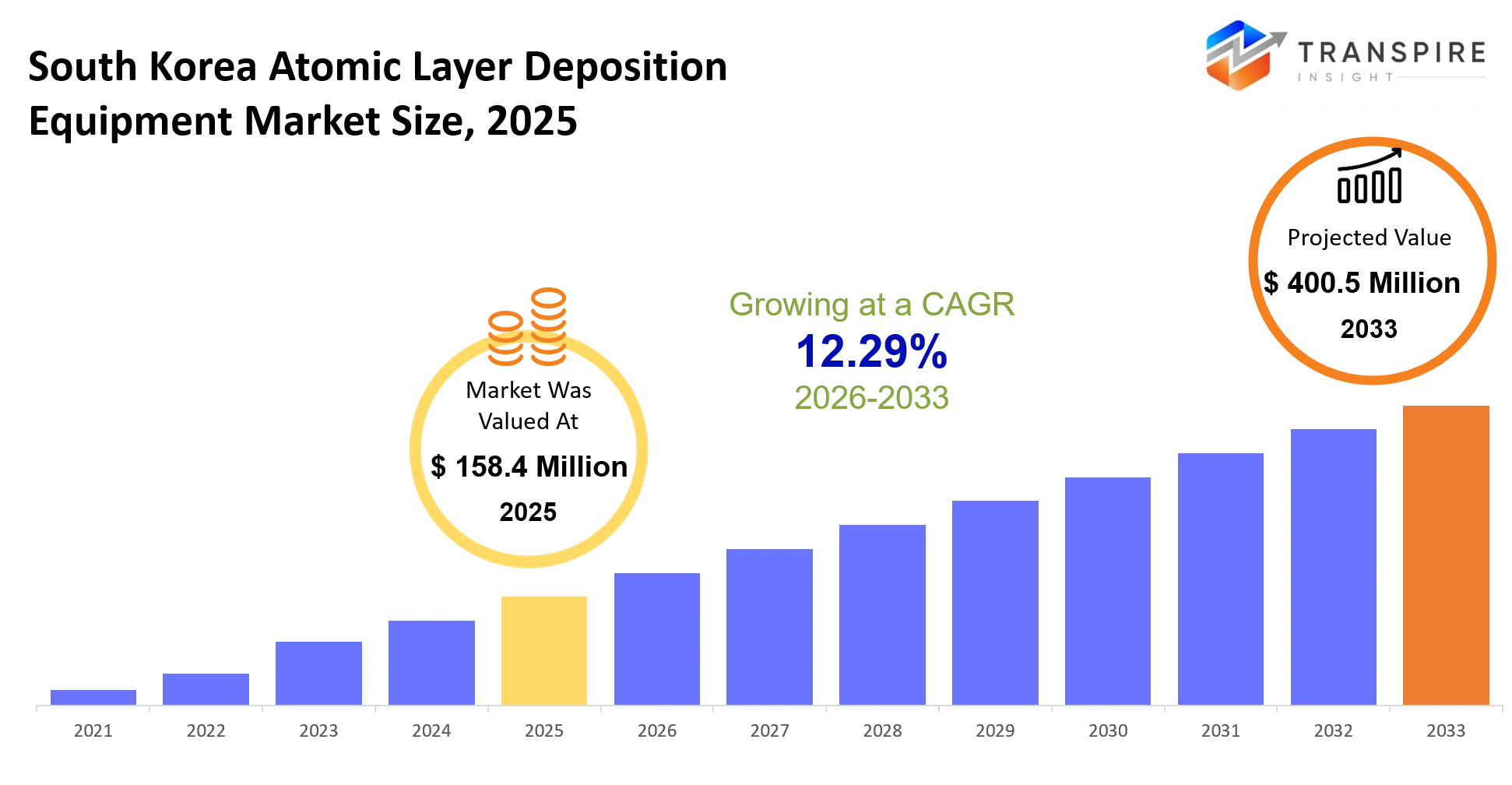
- South Korea Atomic Layer Deposition Equipment Market Size 2025: USD 158.4 Million
- South Korea Atomic Layer Deposition Equipment Market Size 2033: USD 400.5 Million
- South Korea Atomic Layer Deposition Equipment Market CAGR: 12.29%
- South Korea Atomic Layer Deposition Equipment Market Segments: By Equipment Type (Thermal ALD, Plasma Enhanced ALD, Spatial ALD, Roll-to-Roll ALD, Batch ALD, Single Wafer ALD, PEALD Systems, Others); By Application (Semiconductors, Memory Devices, Logic Chips, Displays, Solar Cells, Medical Devices, Advanced Packaging, Others); By End User (Foundries, IDMs, Research Institutes, Display Manufacturers, Solar Companies, Universities, Electronics Firms, Others); By Component (Reactors, Precursors, Pumps, Control Systems, Chambers, Monitoring Systems, Consumables, Others)
South Korea Atomic Layer Deposition Equipment Market Summary
The South Korea Atomic Layer Deposition Equipment Market was valued at USD 158.4 Million in 2025. It is forecast to reach USD 400.5 Million by 2033. That is a CAGR of 12.29% over the period.
The South Korea Atomic Layer Deposition Equipment Market sits right at the center of advanced semiconductor manufacturing, helping chipmakers put down ultra-thin films with atomic-level precision while transistor structures get smaller and more tangled over time. In day to day use, these systems solve a big production problem, they keep coatings uniform in memory chips, logic devices, and the newer semiconductor packages where usual deposition techniques can’t really hold performance steady or protect yield. Over the last three to five years , the market has kinda shifted its gears from flat scaling toward more three dimensional layouts and advanced nodes, so fabrication plants end up investing in smarter deposition tech, even if it takes a bit more planning. That move got an extra push after pandemic era supply chain disruptions, and geopolitical frictions showed where the weak spots really are in sourcing semiconductors, and it also nudged South Korea to back stronger domestic chip manufacturing programs As the fabs grow and device complexity keeps climbing, spending on ALD equipment increasingly mirrors the strategic focus on process accuracy, which then can lead to longer technology upgrade cycles, and yes, better revenue chances for the equipment providers.
Key Market Insights
- The South Korea Atomic Layer Deposition Equipment Market is turning more and more toward advanced memory fabrication, because DRAM and NAND makers moved into those sub-10 nm nodes, not long ago.
- Around Seoul and Suwon there’s this big metropolitan semiconductor cluster, and it basically takes the lion share—close to 65% market share—mostly because fabrication capacity is tightly concentrated and R&D budgets keep getting poured in.
- Central and southern hubs are also rising fast through 2032, with new fabs coming online and government-supported technology initiatives doing the heavy lifting.
- When it comes to system type, Thermal ALD systems currently lead at roughly 45%, since vendors are pushing hardest for uniform thin-film deposition, especially for newer semiconductor structures.
- Plasma-enhanced ALD sits in second place, while spatial ALD is actually the fastest-growing technology, largely because people want higher throughput requirements, and well, they needed it yesterday.
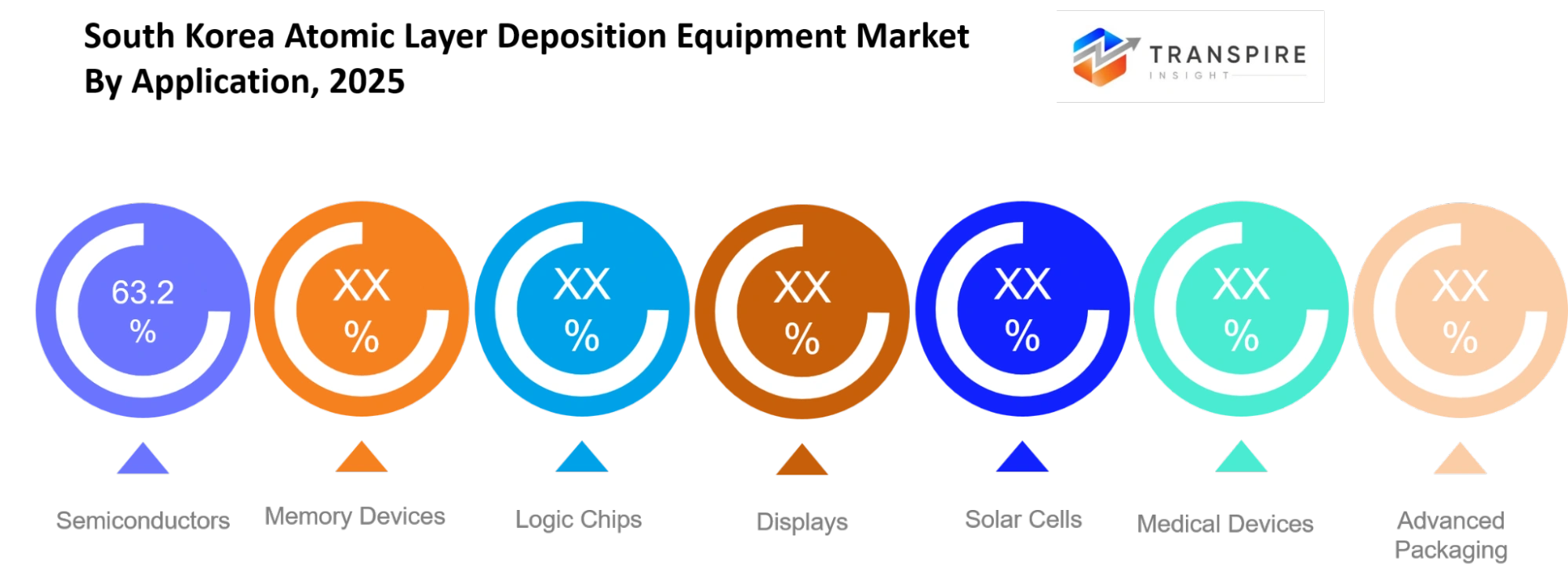
- For applications, semiconductor manufacturing dominates, and it’s well above 75% share. At the same time advanced packaging and heterogeneous integration are showing the quickest adoption rates, kind of like they’re just moving earlier than expected.
- On end users, memory manufacturers are still out front around 60%, whereas foundries and logic chip producers are gathering meaningful growth momentum too.
- Demand really started to shift after 2023, as AI accelerators and high-bandwidth memory drove extra demand for ultra-thin dielectric and conductive films, across the stack.
- Equipment suppliers are also leaning into AI driven process control, which helps boost wafer uniformity improvements by more than 10% when compared with older monitoring setups.
- And since 2024, strategic partnerships between equipment manufacturers and chipmakers ramped up, which shortens technology qualification cycles, and generally improves overall production efficiency.
What are the Key Drivers, Restraints, and Opportunities in the South Korea Atomic Layer Deposition Equipment Market?
The main growth driver is South Korea, where investment in advanced semiconductor manufacturing is really speeding up. This move, toward sub-10 nm memory chips, plus AI accelerators and high-bandwidth memory, makes a pretty specific kind of technical need, atomic scale film deposition, but with exceptional uniformity. Big domestic semiconductor manufacturers are spending heavily on new plants and lines, so equipment procurement is going up too, and since 3D device architectures are taking over, wafers now need more deposition cycles, per single wafer. All of that pretty much pushes equipment revenue higher, and it also helps expand installed production capacity.
Still, the biggest obstacle stays the high cost, and the not-so-simple technology behind ALD systems. The newer deposition tools need sophisticated vacuum chambers, carefully selected precursor chemistries, and precision control systems, which collectively raise acquisition expenses as well as ongoing maintenance costs. This is sort of structural, because qualification cycles in semiconductor fabs are drawn out, and customers tend to be hesitant to switch suppliers. So new entrants don’t just launch faster, they often get delayed commercialization, and in the meantime the market sees slower supplier diversification.
One major opening is advanced packaging and heterogeneous integration. As chipmakers start combining logic, memory, and specialized processors inside a single package, the demand for conformal thin-film deposition keeps climbing. At the same time, investments in chiplet architectures and AI driven semiconductor production are forming a more favorable environment. Suppliers that can build high-throughput ALD platforms, tuned for complex packaging steps, are the ones likely to benefit.
What Has the Impact of Artificial Intelligence Been on the South Korea Atomic Layer Deposition Equipment Market?
Artificial intelligence is kind of reshaping the South Korea Atomic Layer Deposition Equipment Market by tuning process control, boosting equipment reliability, and pushing production efficiency across semiconductor fabs, which is being done in quite a lot of steps. More manufacturers are putting AI style algorithms to work to watch deposition chambers in real time and then making quick adjustments to temperature, precursor flow and plasma conditions so the film stays uniform across wafers. That kind of automation cuts down process deviations and lets teams keep tighter control over semiconductor structures that are getting more and more intricate.
On top of that, machine learning is helping predictive maintenance actually become stronger. Equipment suppliers take sensor information from pumps, valves, and vacuum systems, then they estimate component failures ahead of time, before unplanned shutdowns happen. In practice, these predictive tools let fabs raise uptime, reduce maintenance expenses, and minimize wafer losses tied to unexpected process interruptions. Also, AI driven analytics are used to tune recipe development, which shortens process qualification cycles and helps production ramp up faster for advanced nodes.
Still, AI adoption has limits, and it isn’t always smooth. Bringing machine learning models into legacy deposition equipment needs real investment, plus a lot of historical process data. On top of that, changes in wafer designs, materials, and production environments can lower the model’s accuracy, so full scale deployment becomes harder for manufacturers who want steady performance across multiple fabrication lines.
Key Market Trends
- Semiconductor manufacturers basically shifted pretty aggressively toward sub-10 nm nodes after 2023, sort of meaning they relied more on atomic-scale deposition for complex three dimensional structures, or at least that’s how it looked from the outside.
- AI chip demand also moved purchasing behavior in a different direction, because fabs started caring more about deposition accuracy and throughput, than they cared about picking tools mainly by conventional cost based equipment logic.
- Since 2022, domestic suppliers expanded their R and D spending by over 15% which was aimed at keeping up, with established global deposition equipment manufacturers and their already locked relationships.
- Plasma enhanced ALD adoption picked up speed, as manufacturers wanted faster cycle times, while also chasing better film properties for advanced memory devices, in practice it became a bit of a loop of wanting everything.
- After 2024, strategic collaborations between equipment vendors and chipmakers increased noticeably, and that helped cut down qualification periods for new tech, and also made commercialization come sooner.
- Manufacturers started integrating AI based monitoring systems more and more, these systems sort of automatically tune precursor delivery and chamber conditions while wafers are processed, not just “observe” but also adjust.
- Supply chains became more localized too, as geopolitical uncertainties kept pushing semiconductor companies to diversify equipment sourcing strategies.
- Meanwhile advanced packaging applications emerged faster than expected, because chiplet architectures increased the need for conformal thin films and more precise material engineering, which is never a small detail.
- Competition shifted away from just hardware specifications, toward integrated solutions that combine deposition technology, analytics software, and predictive maintenance capabilities all together.
- And sustainability gained real importance , since equipment makers rolled out energy efficient chambers, plus precursor utilization technologies intended to reduce operational costs.
South Korea Atomic Layer Deposition Equipment Market Segmentation
By Equipment Type:
Thermal ALD relies on heat for getting thin , and very uniform layers onto substrates, and it still remains a favored option where people need really controlled film quality. Plasma Enhanced ALD brings in plasma to boost reaction efficiency, and also to bring processing temperatures down, while Spatial ALD is more about high-speed deposition for large scale production , so it kinda targets throughput.
Roll-to-Roll ALD helps with continuous coating on flexible materials, and it is seeing more adoption in advanced electronics. Batch ALD runs several wafers at once to squeeze out better productivity , whereas Single Wafer ALD gives better precision for advanced semiconductor work. PEALD Systems, and other specialized equipment, provide tailored setups for distinct industrial , as well as research use cases.
By Application:
Semiconductors are a big application area because demand keeps growing for smaller and more efficient electronics. Memory Devices need highly even thin films in order to increase storage density and keep performance solid , while Logic Chips depend on careful deposition techniques to enable advanced computing features.
Displays also use atomic layer deposition to strengthen image quality and durability. Solar Cells can benefit from thin protective coatings that raise energy conversion efficiency. Medical Devices, Advanced Packaging, and other categories keep expanding because manufacturers are actively seeking exact coating methods for tricky products and future electronic systems.
By End User:
Foundries play a role that is pretty big in a practical sense, because they manufacture chips for several customers, and also put a lot of money into advanced deposition technologies. IDMs, on the other hand, combine design with making, so they end up creating strong demand for high performance equipment, right? Research Institutes often bring in new systems so they can back innovation and materials development actions, not just one thing.
Display Manufacturers and Solar Companies also lean on deposition tools, mainly to lift product efficiency and overall performance. Universities contribute too, through research efforts, and more hands on technology development. Meanwhile Electronics Firms fold advanced coating solutions into their manufacturing routines. And other end users keep looking at new uses which should help future market growth in a gradual way.
By Component:
Reactors are basically the key processing units, where thin film deposition happens with controlled conditions and a calm process flow. Precursors give the chemical building blocks that are needed for the layer creation, and pumps keep the vacuum steady so production cycles stay stable and accurate. Control Systems set and regulate operating parameters, plus they make the process consistent across various applications, even when requirements shift.
Chambers form the environment needed for deposition, whereas Monitoring Systems observe how things are going and flag potential problems in real time. Consumables and other support parts still matter a lot, because they help keep equipment efficiency, and they support long term operational reliability.
What are the Key Use Cases Driving the South Korea Atomic Layer Deposition Equipment Market?
Semiconductor manufacturing still feels like the main use case behind the South Korea Atomic Layer Deposition Equipment Market, more or less. Chipmakers depend on atomic layer deposition to build ultra-thin and very consistent films, the kind you need for advanced memory chips as well as logic devices. At the same time, more capital is flowing into AI processors, high-bandwidth memory and ever-smaller transistor designs. So equipment demand keeps climbing, basically.
Display manufacturing and advanced packaging are starting to catch up as secondary applications too. For displays, deposition tech helps boost panel performance, and also durability, it’s kind of a straightforward trade. For electronics, companies adopt deposition and related processing steps in advanced packaging, to make compact devices that still run at high performance, with improved power efficiency.
Then there are the newer, emerging use cases—like medical devices and next-generation solar cells. Some manufacturers are looking at atomically controlled coatings to support better biocompatibility, while solar teams keep pushing advanced thin films to raise energy conversion efficiency and also extend product lifespan over the forecast period.
|
Report Metrics |
Details |
|
Market size value in 2025 |
USD 158.4 Million |
|
Market size value in 2026 |
USD 177.9 Million |
|
Revenue forecast in 2033 |
USD 400.5 Million |
|
Growth rate |
CAGR of 12.29% from 2026 to 2033 |
|
Base year |
2025 |
|
Historical data |
2021 - 2024 |
|
Forecast period |
2026 - 2033 |
|
Report coverage |
Revenue forecast, competitive landscape, growth factors, and trends |
|
Country scope |
South Korea |
|
Key company profiled |
ASM International, Applied Materials, Lam Research, Tokyo Electron, Veeco, Beneq, Oxford Instruments, Jusung Engineering, Wonik IPS, Eugene Technology, Samsung Electronics, SK Hynix, CN1, Picosun, NAURA |
|
Customization scope |
Free report customization (country, regional & segment scope). Avail customized purchase options to meet your exact research needs. |
|
Report Segmentation |
By Equipment Type (Thermal ALD, Plasma Enhanced ALD, Spatial ALD, Roll-to-Roll ALD, Batch ALD, Single Wafer ALD, PEALD Systems, Others); By Application (Semiconductors, Memory Devices, Logic Chips, Displays, Solar Cells, Medical Devices, Advanced Packaging, Others); By End User (Foundries, IDMs, Research Institutes, Display Manufacturers, Solar Companies, Universities, Electronics Firms, Others); By Component (Reactors, Precursors, Pumps, Control Systems, Chambers, Monitoring Systems, Consumables, Others) |
Which Regions are Driving the South Korea Atomic Layer Deposition Equipment Market Growth?
The Seoul metropolitan area still stays the main region in the South Korea Atomic Layer Deposition Equipment Market, mostly because the big semiconductor fabrication facilities , research centers and equipment vendors are basically clustered in that corridor. There is also solid government backing for semiconductor self reliance, and ongoing spending for newer chip production which makes the region lead for longer. Big payments going into memory and logic manufacturing create a pretty steady need for deposition gear and the nearby enabling technologies. Plus, a pretty mature supplier network , a trained workforce , and that close cooperation between makers and universities keep pushing durable growth across the area.
Gyeonggi Province comes next as the second key region, but the way it grows looks a bit different compared with Seoul. Here, the regional expansion leans more toward manufacturing stability and long term industrial funding rather than just having headquarters and research centers all in one place. Ongoing budgets for semiconductor production upgrades, plus strong ties with local supply chains, deliver more dependable revenue chances. Business conditions stay steady and capacity expands little by little, so equipment demand stays supported through the already formed industrial clusters.
The southern region, maybe starting around Busan and Daegu, shows the quickest growth momentum as semiconductor investments steadily roll out beyond the old manufacturing centers. Lately, infrastructure upgrades have been coming in, plus extra backing for advanced technology industries, and also growing desire for diversified production networks. This combo is opening fresh doors. Electronics firms are expanding their manufacturing capacity while research institutions, at the same time, are deepening collaboration with equipment suppliers. Overall growth across this region should bring attractive prospects for market entrants and investors throughout the 2026 to 2033 time window.
Who are the Key Players in the South Korea Atomic Layer Deposition Equipment Market and How Do They Compete?
Competition in the South Korea Atomic Layer Deposition Equipment Market stays pretty moderately concentrated, because a small set of global suppliers goes up against a few specialized domestic manufacturers. In practice, technology innovation still looks like the main thing that drives rivalry. Semiconductor producers want higher precision, faster throughput, and fewer defects, so nobody can really slow down there. At the same time established companies keep defending their market share via steady research efforts, and the domestic players try to move up by delivering tailored approaches, plus quicker customer support.
ASM International puts its attention on advanced thermal and plasma deposition methods, enabling more exact thin film build up for leading-edge semiconductor parts. They keep investing in research, and they also maintain close cooperation with semiconductor manufacturers, which helps ASM shape solutions for next generation chip structures, kind of like on request but faster. Applied Materials differentiates with integrated manufacturing platforms, where deposition, process control, and automation technologies are treated as one, so customers can lift production efficiency and also reduce day-to-day operating expenses.
Tokyo Electron leans into high-throughput systems and relies on deep customer collaboration, to keep up with semiconductor needs that keep shifting. Jusung Engineering competes using specialized deposition technologies and a flexible product development style, which makes it easier to adapt to what customers ask, without too much delay. Wonik IPS, on the other hand, expands its presence by reinforcing domestic partnerships and investing in upgraded equipment design approaches, aimed at supporting memory chips, logic devices, and even newer packaging use cases.
Company List
- ASM International
- Applied Materials
- Lam Research
- Tokyo Electron
- Veeco
- Beneq
- Oxford Instruments
- Jusung Engineering
- Wonik IPS
- Eugene Technology
- Samsung Electronics
- SK Hynix
- CN1
- Picosun
- NAURA
Recent Development News
In May 2026, Jusung Engineering shipped the world's first Atomic Layer Growth (ALG) semiconductor manufacturing equipment to a global chipmaker. The commercialization of ALG technology represents a significant advancement beyond conventional ALD systems and is expected to support next-generation AI semiconductor production while strengthening South Korea’s equipment innovation capabilities. Sourcehttps://en.sedaily.com/
In April 2025, IBM and Tokyo Electron renewed a five-year strategic partnership for advanced semiconductor technology research and development. The collaboration focuses on next-generation semiconductor nodes and chiplet architectures, which will accelerate innovation across deposition, patterning, and advanced manufacturing technologies used throughout the semiconductor value chain. Sourcehttps://newsroom.ibm.com/
What Strategic Insights Define the Future of the South Korea Atomic Layer Deposition Equipment Market?
The South Korea Atomic Layer Deposition Equipment Market is shifting, kinda toward a more specialized and tech intense setup over the next five to seven years. The momentum in growth will rely more on demand for advanced memory, AI accelerators, and heterogeneous integration. Not so much on the usual “just expand capacity” play. Equipment players that can push higher throughput, better material efficiency and add AI assisted process control will sit in a stronger spot as chip designs keep getting more intricate.
There’s also a risk that is harder to see at first, market concentration. A big slice of equipment demand is tied to only a few semiconductor makers, which makes suppliers face swings linked to capital expenditure cycles and procurement choices. If large fab investments get delayed even a little, equipment orders and revenue predictability can feel it fast, and sometimes unexpectedly.
At the same time there’s a newer opening in atomic scale deposition for chiplet packaging and advanced three dimensional architectures. Market participants should start investing early in dedicated deposition platforms, and they should also build development partnerships with semiconductor manufacturers. This is to lock in long term technology adoption, and to help stabilize those future revenue streams.
South Korea Atomic Layer Deposition Equipment Market Report Segmentation
By Equipment Type
- Thermal ALD
- Plasma Enhanced ALD
- Spatial ALD
- Roll-to-Roll ALD
- Batch ALD
- Single Wafer ALD
- PEALD Systems
By Application
- Semiconductors
- Memory Devices
- Logic Chips
- Displays
- Solar Cells
- Medical Devices
- Advanced Packaging
By End User
- Foundries
- IDMs
- Research Institutes
- Display Manufacturers
- Solar Companies
- Universities
- Electronics Firms
By Component
- Reactors
- Precursors
- Pumps
- Control Systems
- Chambers
- Monitoring Systems
- Consumables
Frequently Asked Questions
Find quick answers to common questions.
The South Korea Atomic Layer Deposition Equipment Market size is USD 400.5 Million in 2033.
Key segments for the South Korea Atomic Layer Deposition Equipment Market are By Equipment Type (Thermal ALD, Plasma Enhanced ALD, Spatial ALD, Roll-to-Roll ALD, Batch ALD, Single Wafer ALD, PEALD Systems, Others); By Application (Semiconductors, Memory Devices, Logic Chips, Displays, Solar Cells, Medical Devices, Advanced Packaging, Others); By End User (Foundries, IDMs, Research Institutes, Display Manufacturers, Solar Companies, Universities, Electronics Firms, Others); By Component (Reactors, Precursors, Pumps, Control Systems, Chambers, Monitoring Systems, Consumables, Others).
Major South Korea Atomic Layer Deposition Equipment Market players are ASM International, Applied Materials, Lam Research, Tokyo Electron, Veeco, Beneq, Oxford Instruments, Jusung Engineering, Wonik IPS, Eugene Technology, Samsung Electronics, SK Hynix, CN1, Picosun, NAURA.
The South Korea Atomic Layer Deposition Equipment Market size is USD 158.4 Million in 2025.
The South Korea Atomic Layer Deposition Equipment Market CAGR is 12.29% from 2026 to 2033.
- ASM International
- Applied Materials
- Lam Research
- Tokyo Electron
- Veeco
- Beneq
- Oxford Instruments
- Jusung Engineering
- Wonik IPS
- Eugene Technology
- Samsung Electronics
- SK Hynix
- CN1
- Picosun
- NAURA
About the Authors

Mayur Shinde
I am Mayur Shinde, a Senior Research Analyst at Transpire Insight, specializing in the Automotive & Transportation and Information & Communication Technology (ICT) Industry. My work focuses on analyzing emerging market trends, technological advancements, competitive landscapes, and industry developments to deliver accurate, data-driven insights. I am passionate about transforming complex market information into clear, actionable content that helps businesses, professionals, and decision-makers stay informed and make confident strategic decisions.

Chakradhar Khansole
Chakradhar serves as the Research Director at Transpire Insight, bringing over 8 years of experience in technology, innovation, and strategic market intelligence. He specializes in transforming complex market data into actionable business insights that enable organizations to make informed, growth-oriented decisions. Recognized for his strategic vision and analytical expertise, Chakradhar leads high-impact research initiatives, delivering comprehensive market assessments, competitive intelligence, and forward-looking industry analysis.
Recently Published Reports
-
Apr 2026
3D Optical Profiler Market
3D Optical Profiler Market Size, Share & Analysis Report By Type (Desktop 3D Optical Profiler, and Portable 3D Optical Profiler), By Technology (Confocal Technology, and White Light Interference), By End-Use Industry (Manufacturing, Research Institutions, Automotive, Aerospace and Defense, Medical Devices, and Other), and Geography (North America, Europe, Asia-Pacific, Middle East and Africa, South and Central America), 2021 - 2031
-
Apr 2026
Depth Sensor Market
Depth Sensor Market Size, Share & Analysis Report By Type (Infrared Depth Sensors, Time-of-Flight (ToF) Sensors, Stereo Vision Sensors, Structured Light Sensors, Ultrasonic Depth Sensors), By Application (Automotive, Robotics, Gaming, Consumer Electronics, Industrial Automation, Healthcare, Security & Surveillance, Others), By End Users (Automotive Manufacturers, Consumer Electronics Companies, Healthcare Providers, Industrial Companies, Security Agencies, Gaming Companies, Robotics Companies, Others), and Geography (North America, Europe, Asia-Pacific, Middle East and Africa, South and Central America), 2021 – 2031
-
Apr 2026
Digital Manufacturing Market
Digital Manufacturing Market Size, Share & Analysis Report By Component (Hardware, Software, and Services), By Technology (Robotics, 3D Printing, Internet of Things (IoT), and Others), By Application (Automotive and Transportation, Aerospace and Defense, Consumer Electronics, Industrial Machinery, and Others), By Process Type (Computer-Based Designing, Computer-Based Simulation, Computer 3D Visualization, Analytics, and Others), and Geography (North America, Europe, Asia-Pacific, Middle East and Africa, South and Central America), 2021 – 2031
-
Apr 2026
Digital Visa Services Market
Digital Visa Services Market Size, Share & Analysis Report By Type (Individual Travelers, Group Travelers), By Application (Tourism, Business Travel, Others), and Geography (North America, Europe, Asia-Pacific, Middle East and Africa, South and Central America), 2021 – 2031