

Chemical Vapour Deposition (CVD) Market Summary:
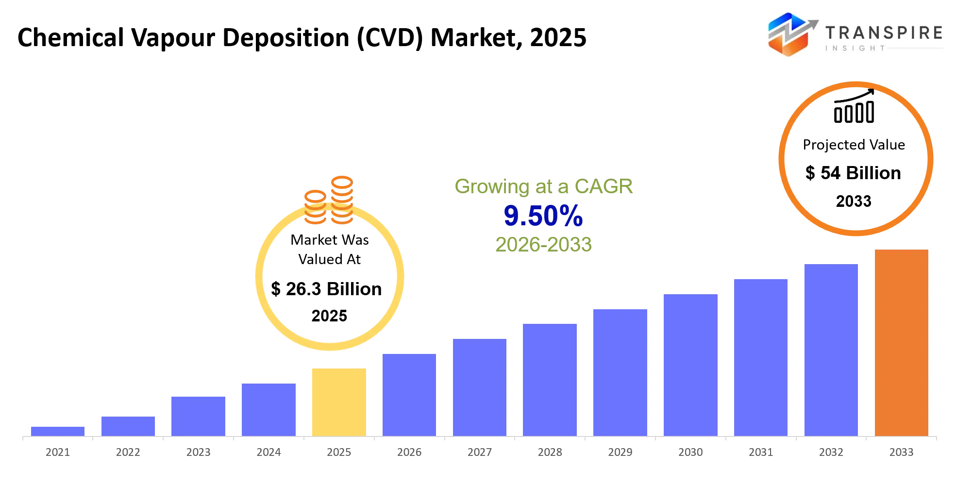
As per the Transpire Insight Analysis, The Chemical Vapour Deposition (CVD) Market size is estimated at USD 26.3 billion in 2025 and is anticipated to reach USD 54 billion by 2033, growing at a CAGR of 9.50% from 2026 to 2033.
The CVD market supplies extremely tightly controlled thin films and functional coatings for building the next generation of semiconductor layers, protecting components and engineering surfaces for highly demanding applications. Between 3 and 5 years ago, the market saw a shift from blanket deposition to low-temperature, selective processes for three-dimensional devices, advanced packaging, compound semiconductors and engineered materials. There is a structural change underway toward atomic-scale process control, as requirements for film uniformity ramp alongside increased silicon and wafer size: that is, high-wafer-transport speeds and wavelength-based layer-thickness dispersion over large areas and bigger substrates. The key driver is the hot growth of AI computing infrastructure, which requires chip companies to achieve 2 nm-class logic, advanced memory and high-bandwidth packaging. The increased adoption of CVD keeps pace with devices reaching a smaller size, which call for more dielectric, barrier, passivation, and epitaxial layers with fewer variations to ensure optimum performance and predictable manufacturing yield. Apart from this, entry into graphene and CVD diamond also opens up the market to other applications besides silicon manufacturing, spreading revenues over all end markets.
Chemical Vapour Deposition (CVD) Market Size & Forecast:
- Market Size 2025: USD 26.3 billion
- Expected Market Value (2033): USD 54 billion
- Forecast CAGR (2026–2033): 9.50%
- Leading Region in 2025: Asia Pacific
- Fastest Growing Region: North America
- Key Company Profiles: Applied Materials, Lam Research, Tokyo Electron, ASM International, Aixtron, Veeco Instruments, CVD Equipment Corporation, Plasma-Therm, IHI Ionbond, Oerlikon Balzers, SENTECH Instruments, Picosun, SPTS Technologies, Kokusai Electric, Jusung Engineering.
Key Chemical Vapour Deposition (CVD) Market Insights:
There is a transition from the separate deposition of films to integrated platforms using artificial intelligence to enhance yield, thermal control, and emissions. The 56% share of Asia Pacific is driven by manufacturing concentration, while new demand is being driven by GaN, advanced memory, optical communications, and thermal-management applications.
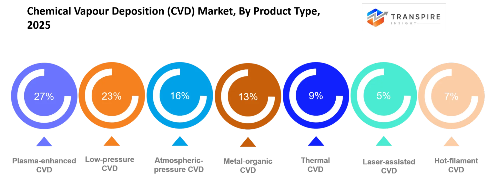
- The semiconductor applications account for 48%, and Applied Materials is making progress in AI-aided PECVD for ultra-thin DRAM and HBM structures.
- With the advent of low-temperature processing in advanced logic and back-end packaging, PECVD is becoming the leading deposition type.
- LPCVD comprises a small 23% of the market, even though it is primarily used for the production of dense, uniform films, as compared to recipe changes.
- Atmospheric-pressure CVD represents 16%, making it a suitable technology for cost-sensitive, higher-throughput industrial coating processes.
- MOCVD accounts for 13%, and AIXTRON's Hyperion 300 mm GaN programme marks a shift to larger wafers and power electronics.
- Thermal CVD represents 9%, and diamond and carbon-based coatings are emerging for high-heat-flux electronics.
- Veeco's Lumina+ batch MOCVD and 300 mm GaN activity have a greater focus on optical communications, micro-LEDs, and power devices.
- While Asia-Pacific dominates with 56%, the North American fabric incentives are shifting to focus more on tool development for supply resilience within the region.
- Periodic inspections are giving way to AI diagnostics, automated handling, and predictive maintenance.
What are the Key Drivers, Restraints, and Opportunities in the Chemical Vapour Deposition (CVD) Market?
Driver:
The expansion of semiconductor capacity is, undoubtedly, the strongest growth driver now. Artificial intelligence servers, high-bandwidth memory, next-generation logic, and 3D NAND require more conformal insulating, conductive, and barrier layers compared to mature planar structures. The combination of AI hardware builds and government incentives favouring domestic fabrication plants in the US, China, and Europe has driven the demand. With higher layer counts and more process complexity, manufacturers buy more chemical vapour deposition chambers, improve cluster platform densities, and will demand faster wafer-handling equipment, all of which naturally lead to higher equipment sales and service revenue.
Restraint:
High capital intensity remains a barrier. Advanced CVD systems require vacuum, gas cabinets, abatement, contamination control, and long customer qualification cycles. Environmental regulations further increase the costs of implementation, as hazardous precursors and high-GWP cleaning gases require monitoring, abatement, and safer options, and these requirements favour existing suppliers and slow adoption in smaller fabrication plants or R&D scale manufacturers.
Opportunity:
Low-temperature PECVD, selective deposition, and intelligent process control can widen CVD use in advanced packaging and thermally sensitive structures. ASM’s PECVD platform supports SiCN for hybrid bonding and stress-tunable SiN for packaging, while AI models are increasingly used to predict film thickness and deposition behaviour. This creates an opportunity for equipment suppliers and fabs to combine automation, advanced materials, and regional semiconductor investment to improve yield and resource efficiency. Regional incentives can accelerate fab investment.
What Has the Impact of Artificial Intelligence Been on the Chemical Vapour Deposition (CVD) Market?
AI is moving chemical vapour deposition away from recipes and toward automated, data-driven process optimization. AI machine learning algorithms can incorporate chamber pressure, gas flow, temperature, plasma conditions, and data from prior wafers to accurately forecast deposition rate, thickness, uniformity, and specification adherence before normal metrology completes. For example, researchers in 2025 used production metrology and a simulation model to forecast silicon nitride deposition rate in plasma-enhanced chemical vapour deposition.
Another 2026 research project applied machine learning to high-density plasma chemical vapour deposition data to predict thin-film thickness across technology nodes. Together, this can enable machine learning for recipe tuning, virtual metrology, anomaly detection, and predictive maintenance, reducing experiments and helping engineers discover process parameters that impact process results. AI can boost efficiency by indicating drift and enabling earlier intervention, before a defect moves through a production lot. The biggest roadblock to AI modelling is data access and quality: models require clean, good data that accurately represents production, and must be robust to changes in recipes, tooling, materials, and process window. Explainability and validation requirements for model use also slow deployment to the fab. Human oversight during deployment is also needed for major recipe adjustments.
In May 2026, partnered with TSMC at the EPIC Centre in Silicon Valley to accelerate materials engineering, equipment innovation, and process integration technologies for next-generation AI semiconductors. This collaboration strengthens the R&D pipeline for advanced deposition and data-driven process solutions as manufacturing complexities escalate.
Key Chemical Vapour Deposition (CVD) Market Trends:
The shift from stand-alone deposition to intelligent, multi-chamber manufacturing platforms is underway for CVD. The competitive edge is moving from the mere deposition of films to control of uniformity, yield, emissions, and uptime in increasingly complex devices.
- Conformal layers are replacing blanket films for GAA transistors, 3D NAND and advanced packaging.
- Conventional CVD is now being combined with ALD: ALD for ultra-thin interfaces, and CVD for productive bulk-film growth.
- Where delicate substrates and back-end structures are concerned, PECVD is gaining traction.
- Recipe tuning, a process of using AI, is scaling from lab to supervised fab optimisation and quality monitoring.
- As sensors reveal chamber fouling and component wear earlier, predictive maintenance is taking the place of calendar-based maintenance.
- Wafer loading, transfer and contamination-controlled handling are now commonplace in PECVD lines and are being automated.
- As the electric vehicle industry and renewable energy and high-frequency electronics continue to grow, SiC and GaN deposition is becoming increasingly strategic.
- Lower GWP precursors and better abatement and less chamber-cleaning emissions are being driven by green-fab requirements.
- CVD diamond is moving from speciality coating applications to thermal management applications in high-power RF and semiconductor packages.
Chemical Vapour Deposition (CVD) Market Segmentation
By Type:
Plasma-enhanced CVD leads at 27%, followed by Low-pressure CVD at 23% and Atmospheric-pressure CVD at 16%, reflecting its importance in controlled semiconductor processing. Metal-organic CVD accounts for 13% and is projected to grow at a 9.8% CAGR, supported by compound semiconductor and optoelectronic manufacturing. Thermal CVD represents 9%, Laser-assisted CVD 5%, Hot-filament CVD 4%, and Others 3%, serving specialized coating, materials engineering, and advanced electronic applications.
By Material:
Carbide and Silicon Nitride remain important for high-temperature, insulating, and semiconductor applications, while Graphene and Diamond expand CVD into advanced thermal and electronic materials. Gallium Nitride supports power electronics and high-frequency devices, strengthening its strategic relevance. Carbon Nanotubes contribute to specialized conductive structures, while Metal Oxides address sensing, dielectric, and protective requirements. Others include emerging engineered materials, creating opportunities for application-specific deposition processes.
By Application:
Semiconductors lead with 48%, reflecting CVD's central role in dielectric, barrier, passivation, and functional thin-film formation. Solar Cells extend adoption into energy-generation technologies, while MEMS require precisely controlled films for miniature sensing and actuation structures. Cutting Tools use CVD coatings for surface durability, while Optical Devices, Medical Devices, Aerospace, and Others create specialised opportunities where thermal stability, wear resistance, electrical performance, and surface protection are critical.
By Equipment:
Hot-wall and Cold-wall systems address different thermal management and contamination-control requirements, while Horizontal and Vertical configurations support distinct wafer-loading and process architectures. Batch systems prioritize throughput for compatible production flows, whereas Single-wafer systems emphasize tighter uniformity and process control. Continuous systems support specialized high-volume applications, while Others serve customized production requirements. Equipment selection increasingly depends on substrate geometry, temperature sensitivity, throughput targets, and film uniformity.
By Substrate:
Silicon remains foundational because of its established semiconductor manufacturing infrastructure and compatibility with mature CVD processes. Glass supports displays, optical components, and functional coatings, while Metal and Ceramic substrates serve demanding thermal and mechanical applications. Polymer enables lower-temperature and flexible applications, whereas Sapphire supports optoelectronics and specialized devices. Compound Semiconductor substrates address GaN and other advanced technologies, while Others accommodate emerging materials requiring customized deposition conditions.
By End User:
Semiconductor remains central because advanced chips require precisely engineered thin films throughout fabrication. Electronics expands CVD use across components and functional surfaces, while Solar supports energy-related applications. Automotive adoption is linked to power electronics, sensors, and durable components, while Aerospace requires high-performance protective materials. Healthcare uses specialised coatings and devices, and Energy benefits from thermal and conductive materials. Others provide additional opportunities across industrial applications and emerging technologies.
By Coating:
Conductive films support electrical pathways and functional surfaces, while Insulating coatings provide dielectric separation within electronic structures. Protective and Wear-resistant coatings improve component durability under mechanical or environmental stress, while Thermal coatings address heat-management requirements. Optical films control transmission, reflection, or related properties, and Barrier coatings limit moisture, gases, or chemical interaction. Others serve specialised requirements, indicating that future CVD adoption will increasingly favour application-specific coating performance.
What are the Key Use Cases Driving the Chemical Vapour Deposition (CVD) Market?
The primary application is semiconductor manufacturing, which accounts for 48% of all applications. CVD is used to generate insulating dielectrics, conductive films, spacers, liners, and barrier layers used in advanced logic, memory, and packaging applications. With the proliferation of 3D structures, additional deposition steps are required per wafer.
Applications are growing rapidly, such as passivation for solar cells, anti-reflective layers, micro-electromechanical systems (MEMS) structures, optical coatings, and wear-resistant coatings for cutting tools, which rely on CVD for precise control of film thickness, adhesion, and performance on speciality substrates.
Emerging applications include SiC and GaN power devices, CVD diamond heat spreaders for high power packages, graphene and CNT films, coatings for aerospace and medical applications, and recent advances in CVD diamond for RF, optoelectronic and semiconductor thermal management.
|
Report Metrics |
Details |
|
Market size value in 2025 |
USD 26.3 Billion |
|
Market size value in 2026 |
USD 28.6 Billion |
|
Revenue forecast in 2033 |
USD 54 Billion |
|
Growth rate |
CAGR of 9.50% from 2026 to 2033 |
|
Base year |
2025 |
|
Historical data |
2021 - 2024 |
|
Forecast period |
2026 - 2033 |
|
Report coverage |
Revenue forecast, competitive landscape, growth factors, and trends |
|
Regional scope |
United States; Canada; Mexico; United Kingdom; Germany; France; Italy; Spain; Denmark; Sweden; Norway; China; Japan; India; Australia; South Korea; Thailand; Brazil; Argentina; South Africa; Saudi Arabia; United Arab Emirates |
|
Key companies profiled |
Applied Materials, Lam Research, Tokyo Electron, ASM International, Aixtron, Veeco Instruments, CVD Equipment Corporation, Plasma-Therm, IHI Ionbond, Oerlikon Balzers, SENTECH Instruments, Picosun, SPTS Technologies, Kokusai Electric, Jusung Engineering. |
|
Customization scope |
Free report customization (country, regional & segment scope). Available customised purchase options to meet your exact research needs. |
|
Report Segmentation |
By Type (Plasma-enhanced CVD, Low-pressure CVD, Atmospheric-pressure CVD, Metal-organic CVD, Laser-assisted CVD, Thermal CVD, Hot-filament CVD, Others); By Material (Silicon Carbide, Silicon Nitride, Graphene, Diamond, Gallium Nitride, Carbon Nanotubes, Metal Oxides, Others); By Application (Semiconductors, Solar Cells, MEMS, Cutting Tools, Optical Devices, Medical Devices, Aerospace, Others); By Equipment (Hot-wall CVD, Cold-wall CVD, Horizontal CVD, Vertical CVD, Batch CVD, Single-wafer CVD, Continuous CVD, Others); By Substrate (Silicon, Glass, Metal, Ceramic, Polymer, Sapphire, Compound Semiconductor, Others); By End User (Semiconductor, Electronics, Solar, Automotive, Aerospace, Healthcare, Energy, Others); By Coating (Conductive, Insulating, Protective, Wear-resistant, Thermal, Optical, Barrier, Others). |
Which Regions are driving chemical vapour deposition (CVD) Market Growth?
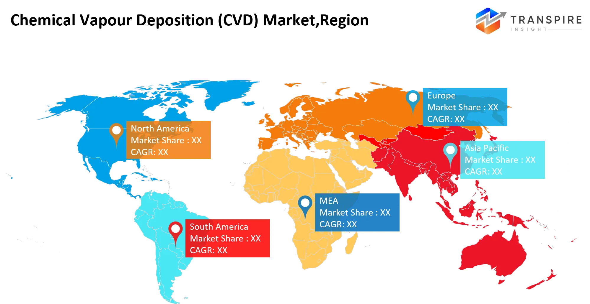
Asia-Pacific dominates, producing 56% of all chips sold in the world, notably because of the location of wafer fabs, memory, display, and compound-semiconductor manufacturing in Taiwan, South Korea, China, and Japan. It has a local supplier base, established foundries, process engineers, high electronics demand, and the desire to use local equipment, with China's domestic focus and Japan's high-quality materials base. Both new-build and established production lines that want to replace old equipment will buy CVD systems.
In September 2026, Samsung Electronics announced a strategic partnership with Mistral AI to implement on-premises AI technologies across its semiconductor operations. This collaboration integrates intelligence-driven infrastructure to optimise chip manufacturing processes.
http://news.samsungsemiconductor.com/global/category/news/
Europe is 17% by comparison. Its growth is not so much volume-driven as it is related to automotive power electronics, industrial automation, photonics, and dedicated research infrastructure. European initiatives in semiconductors, automotive decarbonisation, and strong equipment engineering give stability while cyclical demand from consumer electronics wanes. As a result, AIXTRON, SENTECH and others are competing on process capability, application labs and specialised compound-semiconductor expertise.
In July 2026, Infineon Technologies opened its Smart Power Fab in Dresden several months ahead of schedule. This €5 billion plant doubles the company's 300mm manufacturing capacity at the site to address surging power semiconductor demand for AI data centres and automotive applications.
https://www.infineon.com/press-release/2026/infxx202606-117
North America accounts for 20% and is forecast to grow at a CAGR of 7.9%, making it the most rapidly growing region in the forecast. The recent change is a result of a policy-driven shift to domestic semiconductor capacity, the funding of AI chips and advanced packaging, which opens up local opportunities for chemical vapour deposition supply chains, high-value service contracts, silicon carbide/gallium nitride manufacturing and software-enabled process control. Latin America and the Middle East and Africa account for 7% as they primarily provide long-term assembly, solar and energy-project opportunities, rather than front-end scale.
In April 2026, Resonac Holdings Corporation launched the US-JOINT advanced semiconductor packaging R&D and evaluation centre in Union City, California. This initiative accelerates commercialisation for generative AI and computing demands by reducing proof-of-concept timelines.
https://www.resonac.com/news/2026/04/20/3803.html
Who are the Key Players in the Chemical Vapour Deposition (CVD) Market, and how do they compete?
Competition in the industry can be divided among large-volume semiconductor platforms, dedicated compound-semiconductor specialists, and precision-coatings providers. Applied Materials, Lam Research, Tokyo Electron, ASM International and Kokusai Electric compete through process integration, throughput, installed-base services and advanced logic/memory capabilities. AIXTRON, Veeco Instruments, Jusung Engineering and Plasma-Therm differentiate through MOCVD, GaN, LED, RF and plasma-processing-related niches, while numerous smaller firms participate in the research, coatings and customised-system segments.
Applied Materials combines process innovations with fab-wide integration, using AI-enabled PECVD and metrology for improved advanced-memory and logic process control. Lam Research emphasises dielectric gap-fill, barrier and metal-deposition applications, and is strengthened by partnerships in materials. Tokyo Electron contributes technology solutions for low-energy plasma, diagnostics and high-volume integration, while ASM International focuses on atomic-scale innovations and advanced gate-stack applications. AIXTRON and Veeco are making acquisitions in micro-LED, Photonics, GaN, and 300 mm platforms; Veeco's Lumina+ and GaN placements are driven by application focus. CVD Equipment Corporation, SENTECH, Picosun and SPTS Technologies serve flexible R&D-to-production niches. IHI Ionbond and Oerlikon Balzers cater to industrial coatings, with Plasma-Therm and Jusung building customised, regional support capabilities.
Key Players are:
- Applied Materials
- Lam Research
- Tokyo Electron
- ASM International
- Aixtron
- Veeco Instruments
- CVD Equipment Corporation
- Plasma-Therm
- IHI Ionbond
- Oerlikon Balzers
- SENTECH Instruments
- Picosun
- SPTS Technologies
- Kokusai Electric
- Jusung Engineering
Recent Development News
In April 2026, ACM Research shipped its first plasma-enhanced chemical vapour deposition (PECVD) silicon carbonitride system to a leading semiconductor manufacturer. The three-station deposition architecture is designed for advanced BEOL and packaging applications, supporting tighter film control, process stability, and uniformity.
In June 2026, Veeco Instruments received commercial acceptance and qualification for its new LUMINA+ metal-organic chemical vapour deposition (MOCVD) system from Ennostar. The system is being deployed for high-volume production of advanced arsenide and phosphide optoelectronic devices, strengthening CVD equipment capabilities for high-throughput compound semiconductor manufacturing.
What Strategic Insights Define the Future of the Chemical Vapour Deposition (CVD) Market?
The CVD market is evolving toward highly selective, low-temperature, and data-optimised deposition. The value is migrating from standalone CVD tools toward integrated process solutions for 3D logic, HBM, advanced packaging, and compound semiconductors. An underappreciated risk in this direction is process fragmentation; the creation of new materials, new substrates, and new architectures prolongs qualification cycles, creates more complex precursors, and diminishes recipe portability across tools. An emerging opportunity is combining CVD with artificial intelligence-powered virtual metrology and selective CVD; it reduces experimental iterations for fabrication plants and has some ability to control a narrowing process window. Opportunities also include CVD-enabled thermal and protective materials for artificial intelligence equipment, power electronics, and next-generation aerospace applications. From a strategic perspective, CVD suppliers should build modular platforms, application-specific process libraries, and foster co-development with fabrication facilities rather than simply growing the installed base. Local fabrication programs highlight the importance of local service, spare parts, and application engineers as differentiators during ramp-up of new or next-generation fabrication plants.
Key Segmentations are:
By Type
- Plasma-enhanced CVD
- Low-pressure CVD
- Atmospheric-pressure CVD
- Metal-organic CVD
- Laser-assisted CVD
- Thermal CVD
- Hot-filament CVD
- Others
By Material
- Silicon Carbide
- Silicon Nitride
- Graphene
- Diamond
- Gallium Nitride
- Carbon Nanotubes
- Metal Oxides
- Others
By Application
- Semiconductors
- Solar Cells
- MEMS
- Cutting Tools
- Optical Devices
- Medical Devices
- Aerospace
- Others
By Equipment
- Hot-wall CVD
- Cold-wall CVD
- Horizontal CVD
- Vertical CVD
- Batch CVD
- Single-wafer CVD
- Continuous CVD
- Others
By Substrate
- Silicon
- Glass
- Metal
- Ceramic
- Polymer
- Sapphire
- Compound Semiconductor
- Others
By End User
- Semiconductor
- Electronics
- Solar
- Automotive
- Aerospace
- Healthcare
- Energy
- Others
By Coating
- Conductive
- Insulating
- Protective
- Wear-resistant
- Hermal
- Optical
- Barrier
- Others
Frequently Asked Questions
Find quick answers to common questions.
The chemical vapour deposition (CVD) market size was valued at USD 26.3 billion in 2025 and is poised to reach USD 54 billion by 2033, expanding at a 9.50% CAGR.
Key segments for the chemical vapour deposition (CVD) market are By Type (Plasma-enhanced CVD, Low-pressure CVD, Atmospheric-pressure CVD, Metal-organic CVD, Laser-assisted CVD, Thermal CVD, Hot-filament CVD, Others); By Material (Silicon Carbide, Silicon Nitride, Graphene, Diamond, Gallium Nitride, Carbon Nanotubes, Metal Oxides, Others); By Application (Semiconductors, Solar Cells, MEMS, Cutting Tools, Optical Devices, Medical Devices, Aerospace, Others); By Equipment (Hot-wall CVD, Cold-wall CVD, Horizontal CVD, Vertical CVD, Batch CVD, Single-wafer CVD, Continuous CVD, Others); By Substrate (Silicon, Glass, Metal, Ceramic, Polymer, Sapphire, Compound Semiconductor, Others); By End User (Semiconductor, Electronics, Solar, Automotive, Aerospace, Healthcare, Energy, Others); By Coating (Conductive, Insulating, Protective, Wear-resistant, Thermal, Optical, Barrier, Others).
th is primarily driven by advanced semiconductor fabrication, 3D device architectures, AI-driven chip production, compound-semiconductor manufacturing, advanced packaging, and adoption of low-temperature and selective deposition technologies.
The chemical vapour deposition (CVD) market is led by major manufacturers, including Applied Materials, Lam Research, Tokyo Electron, ASM International, Aixtron, Veeco Instruments, CVD Equipment Corporation, Plasma-Therm, IHI Ionbond, Oerlikon Balzers, SENTECH Instruments, Picosun, SPTS Technologies, Kokusai Electric, and Jusung Engineering.
Asia Pacific holds 56% of the market, supported by major semiconductor manufacturing hubs, advanced fabrication infrastructure, government-backed investments, and strong demand for deposition equipment across China, Taiwan, South Korea, and Japan.
Commercial opportunities include selective and low-temperature deposition, AI-enabled process optimisation, advanced packaging, compound semiconductors, CVD diamond, graphene, and localised equipment supply for new semiconductor fabs.
- Applied Materials
- Lam Research
- Tokyo Electron
- ASM International
- Aixtron
- Veeco Instruments
- CVD Equipment Corporation
- Plasma-Therm
- IHI Ionbond
- Oerlikon Balzers
- SENTECH Instruments
- Picosun
- SPTS Technologies
- Kokusai Electric
- Jusung Engineering
About the Authors

Pankaj Ghogare Patil
I am Pankaj Ghogare Patil, a Senior Research Analyst at Transpire Insight, specializing in the Pharmaceutical, Chemicals & Materials, Healthcare IT, and Biotechnology industry. My expertise lies in conducting comprehensive market research, analyzing industry trends, evaluating competitive landscapes, and translating complex data into actionable insights. At Transpire Insight, I closely follow emerging technologies, regulatory developments, and market innovations to create accurate, well-researched, and informative content that helps businesses and professionals make informed decisions. I am committed to producing credible, evidence-based articles that reflect industry best practices while making technical topics accessible and valuable for a broad audience.

Chakradhar Khansole
Chakradhar serves as the Research Director at Transpire Insight, bringing over 8 years of experience in technology, innovation, and strategic market intelligence. He specializes in transforming complex market data into actionable business insights that enable organizations to make informed, growth-oriented decisions. Recognized for his strategic vision and analytical expertise, Chakradhar leads high-impact research initiatives, delivering comprehensive market assessments, competitive intelligence, and forward-looking industry analysis.
Recently Published Reports
-
May 2026
Healthcare Polymer Packaging Market
Healthcare Polymer Packaging Market Size, Share & Analysis Report By Packaging Type (Syringes, IV Bottles and Pouches, Clamshells, Blisters, Bottles & Jars, Containers, Tubes, IV Parental Packaging, Others), By Type (Regulated, Non-regulated), By Polymer Type (LDPE (Low-Density Polyethylene), HDPE (High-Density Polyethylene), Homo-polymer (Homo), Random Copolymer (Random), Block Copolymer (Block), PET, Polystyrene, Polyvinyl Chloride, Polyamide/EVOH, Others), and Geography (North America, Europe, Asia-Pacific, Middle East and Africa, South and Central America), 2021 - 2031
-
Apr 2026
Hydrophilic Tape (Waterstop) Market
Hydrophilic Tape (Waterstop) Market Size, Share & Analysis Report By Type (Bentonite-Based Hydrophilic Tape, Rubber-Based Hydrophilic Tape), By Application (Residential Buildings, Commercial Buildings, Infrastructure Projects), and Geography (North America, Europe, Asia-Pacific, Middle East and Africa, South and Central America), 2021 - 2031
-
Apr 2026
Metalens Market
Metalens Market Size, Share & Analysis Report By Type (Visible Light Metalens, and Infrared Metalens), By Application (Consumer Electronics, Automotive Electronics, Industrial, Medical, and Others), and Geography (North America, Europe, Asia-Pacific, Middle East and Africa, South and Central America), 2021 - 2031
-
Apr 2026
PBT Resin Market
PBT Resin Market Size, Share & Analysis Report By Type (Reinforced PBT Resin, Unreinforced PBT Resin), By Processing Method (Injection Molding, Extrusion, Blow Molding, Others), By End-User (Automotive, Electrical & Electronics, Consumer Appliances, Industrial Machinery, Medical Devices, Packaging, Others), and Geography (North America, Europe, Asia-Pacific, Middle East and Africa, South and Central America), 2021 - 2031