
Aug 03, 2026
By Transpire Insight
Description
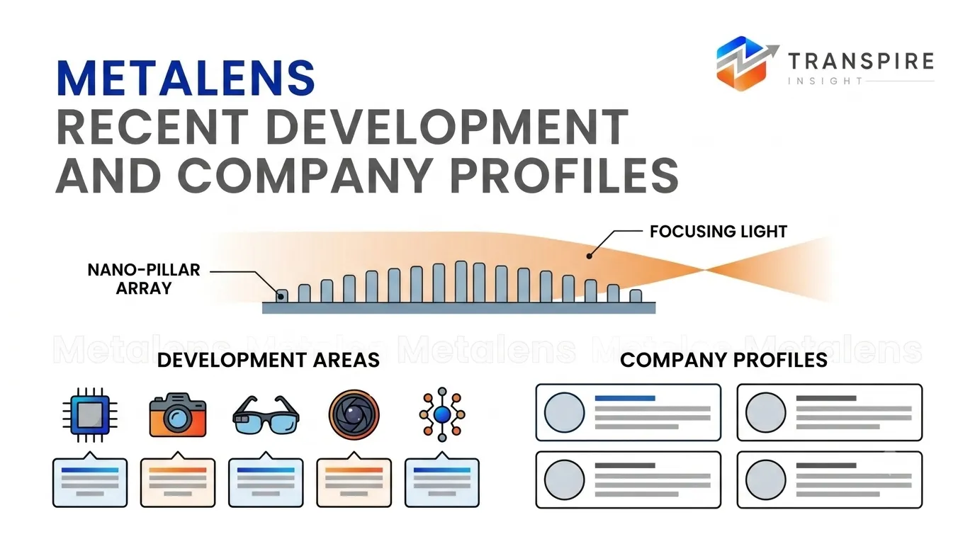
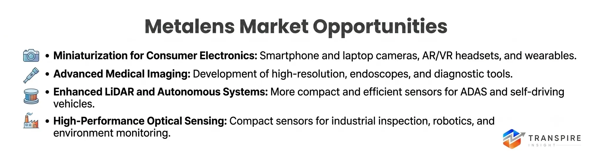
According to a research report published by Transpire Insight, The Metalens Market size is projected to Grow from USD 47.6 Million in 2025 to USD 1852.4 Million by 2035, at a CAGR of 68% during the forecast period 2026-2035. Market expansion is influenced by the rise in the demand for micro-optics, quick adaptation of AR/VR technologies, 3D sensing, LiDARs, computational photography, and improved camera modules in smartphones. The constant development of nanofabrication, metasurface technology, semiconductor fabrication techniques, and photonic integration is making commercial applications easier and faster. In addition to this, the rising interest in autonomous mobility, diagnostics, space optics, and high-performance sensors will provide immense future prospects to the Metalens Market.
Introduction
The Metalens Market covers the design and deployment of ultrathin optical lenses developed by utilizing nanostructured metasurfaces instead of traditional curved optical lenses which are made up of either glass or plastic materials. Metalenses can control light at the nanoscale level and provide an optical system which is compact and flexible in order to be used in applications such as consumer electronics, smartphones, AR, VR, autonomous cars, medical imaging, aerospace, defense, LiDAR and industrial sensing.
Recent Development News
Stay Ahead of Emerging Opportunities with Expert Market Insights by Transpire Insight
The insights that have been shared through this blog are based on intensive market research carried out by Transpire Insight, an advisor that works with many organizations. Thanks to the analysis of extensive data, forecasts made by our specialists, and industry intelligence, our reports allow clients to find strategic growth opportunities in dynamically developing industries. For all those who would like to get more detailed information regarding market segmentation, competitive analysis, regional outlooks, and future investment tendencies, there is no doubt that our full report will be of great value.
Download the exclusive Metalens Market sample report today to uncover expert insights, emerging trends, and the opportunities defining the future of the industry.
Metalens Market Size & Statistics
Regional Growth and Demand Analysis by Transpire Insight:
The Metalens Market is led by North America, which holds about 41% of the total share in the Metalens Market. The dominance of North America in the Metalens Market can be attributed to the region's robust ecosystem of semiconductor firms, nanophotonics research facilities, defense technology providers, and advanced consumer electronics manufacturers. The investments in metasurface optics, computational imaging, LiDAR, augmented reality (AR), virtual reality (VR), autonomous cars, and biomedical imaging are high in the region. Besides, the region has an abundance of pioneering companies like Metalenz, and the partnerships between universities and industries and the considerable funding from both the public and private sectors for photonics are aiding the commercialization process. The fast adoption of next-generation sensing technologies in aerospace, defense, and healthcare sectors is driving the growth of North America in the Metalens Market.
Fastest growing region: The Asia-Pacific region is expected to register the fastest growth rate during the forecast period owing to the rapid growth in semiconductor production, smartphone production, AR/VR devices production, consumer electronics production, and investments in photonics technologies in China, Japan, South Korea, and Taiwan.
Top 15 Trends in the Metalens Market
Proceed to Checkout to purchase the exclusive Metalens Market report and gain instant access to in-depth market intelligence, strategic analysis, and future growth opportunities.
1. Growing Adoption of Metalenses in Smartphone Cameras
There is an ongoing incorporation of metalenses in smartphones to decrease the size of camera modules and improve optical performance. The reason behind this is the smaller optical design, thinning of camera modules, better image resolution, reduced manufacturing complexity, depth sensing, and the development of next-generation mobile devices.
2. Expansion of AR and VR Optical Applications
The metalenses are becoming a key part of augmented and virtual reality gadgets by providing light and compact optical systems that can produce highly accurate images. The reduction in weight of headsets, clarity in images produced, broader field of view, comfort for users, optical efficiency, and increasing usage of immersive technologies by consumers are driving market growth.
3. Increasing Integration of Metalenses in LiDAR Systems
Metalens is being used by the automotive industry and industries for the improvement of performance in LiDAR systems along with downsizing the system. Better sensing accuracy, smaller sensor design, reduced weight, enhanced autonomy in navigation, scalability in production, and an increase in autonomous vehicles are some reasons for this trend.
4. Rising Demand for Miniaturized Optical Components
The current trend of shrinking devices in consumer electronics, health care, and industrial applications has created demand for ultra-thin metalenses. Smaller size of products, light optical system, flexible design, easy integration, portability, and efficient manufacturing processes have been key drivers for the growth of the market.
5. Growth of Computational Imaging Technologies
Metalenses are being used extensively in computational imaging platforms to improve image processing capability while reducing hardware complexity. This is mainly because of improved image reconstruction, increased optical accuracy, reduction in hardware needs, increased capability of image processing by artificial intelligence, increased flexibility, and the increasing need for intelligent vision systems.
6. Development of CMOS-Compatible Metalens Manufacturing
CMOS-compatible processes for mass production of metalenses through existing semiconductor fabrication technologies are currently being developed by manufacturers. The increasing demand for metalenses can be attributed to reduced cost of production, scalability in manufacturing, easy integration with image sensors, fast commercialization, better product consistency, among others.
Top 25 Companies Leading the Metalens Market
Customize the exclusive Metalens Market report today to receive tailored insights, country-specific analysis, and business-focused market intelligence.
1. Metalenz Inc.
Metalenz Inc. is a photonics company commercializing metasurface optics (metalenses) for consumer electronics, automotive sensing, and biometric applications.
Founded:2016 | Headquarters: Boston, Massachusetts, USA
Why It Ranks: Pioneer in commercial metalens technology with high-volume semiconductor integration.
Regional Dominance: Strong presence across North America, Europe, and Asia-Pacific.
Product Line: Metalenses, Polar ID™, Polar 3D™, Optical Sensing Solutions, and Metasurface Optics.
Recent Development: Expanded commercialization of under-display metalens-based biometric authentication solutions.
2. MetaOptics Ltd.
MetaOptics develops advanced metasurface optical technologies for imaging, sensing, and next-generation consumer electronics.
Founded:2020 | Headquarters: Singapore
Why It Ranks: Emerging innovator in CMOS-compatible metalens manufacturing.
Regional Dominance: Strong presence across Asia-Pacific, Europe, and North America.
Product Line: Metalenses, AR/VR Optical Components, Smartphone Optics, and Imaging Modules.
Recent Development: Expanded international customer evaluation programs for metalens-enabled devices.
3. NIL Technology ApS
NIL Technology specializes in nanophotonics, nanoimprint lithography, and advanced metasurface optical components.
Founded:2006 | Headquarters: Kongens Lyngby, Denmark
Why It Ranks: Leading developer of metalenses and nano-optical solutions.
Regional Dominance: Strong presence across Europe, North America, and Asia-Pacific.
Product Line: Metalenses, Diffractive Optics, Nanoimprint Lithography Solutions, Optical Components, and LiDAR Optics.
Recent Development: Expanded production capabilities for advanced metasurface optical products.
4. Lumotive Inc.
Lumotive develops programmable optical semiconductor technologies for LiDAR, 3D sensing, and machine vision applications.
Founded:2018 | Headquarters: Redmond, Washington, USA
Why It Ranks: Innovator in solid-state beam steering using metasurface technology.
Regional Dominance: Strong presence across North America and Asia-Pacific.
Product Line: Optical Semiconductors, Beam Steering Chips, LiDAR Components, and Metasurface Optical Systems.
Recent Development: Expanded partnerships for automotive and industrial sensing platforms.
5. Samsung Electronics Co., Ltd.
Samsung Electronics is a technology company manufacturing semiconductors, smartphones, displays, and advanced imaging solutions.
Founded:1969 | Headquarters: Suwon, South Korea
Why It Ranks: Major investor in next-generation optical and semiconductor technologies.
Regional Dominance: Strong presence across Asia-Pacific, North America, and Europe.
Product Line: Smartphone Camera Modules, Semiconductor Chips, Image Sensors, Optical Components, and Consumer Electronics.
Recent Development: Continued investment in advanced imaging technologies incorporating metasurface research.
6. Sony Group Corporation
Sony develops consumer electronics, semiconductor image sensors, entertainment technologies, and advanced optical systems.
Founded:1946 | Headquarters: Tokyo, Japan
Why It Ranks: leader in CMOS image sensor technology.
Regional Dominance: Strong presence across Asia-Pacific, Europe, and North America.
Product Line: CMOS Image Sensors, Optical Modules, Camera Systems, Imaging Semiconductors, and Electronics.
Recent Development: Expanded advanced image sensor technologies supporting next-generation optics.
7. Canon Inc.
Canon manufactures cameras, imaging equipment, optical devices, semiconductor equipment, and industrial systems.
Founded:1937 | Headquarters: Tokyo, Japan
Why It Ranks: Long-standing leader in precision optical technologies.
Regional Dominance: Strong presence across Asia-Pacific, Europe, and North America.
Product Line: Cameras, Optical Lenses, Semiconductor Lithography Equipment, Medical Imaging Systems, and Industrial Optics.
Recent Development: Continued investment in advanced photonics and precision optical manufacturing.
8. Nikon Corporation
Nikon develops precision optical equipment, cameras, microscopes, semiconductor manufacturing systems, and imaging technologies.
Founded:1917 | Headquarters: Tokyo, Japan
Why It Ranks: Major innovator in precision optics and semiconductor lithography.
Regional Dominance: Strong presence across Asia-Pacific, Europe, and North America.
Product Line: Optical Lenses, Semiconductor Lithography Systems, Cameras, Microscopes, and Precision Instruments.
Recent Development: Expanded advanced semiconductor manufacturing technologies supporting photonics innovation.
9. STMicroelectronics N.V.
STMicroelectronics manufactures semiconductor devices serving automotive, industrial, consumer electronics, and sensing applications.
Founded:1987 | Headquarters: Geneva, Switzerland
Why It Ranks: Leading semiconductor manufacturer integrating metalens technologies into sensing platforms.
Regional Dominance: Strong presence across Europe, Asia-Pacific, and North America.
Product Line: Image Sensors, MEMS Devices, Microcontrollers, Optical Sensors, and Semiconductor Components.
Recent Development: Expanded commercialization of metasurface-based optical sensing technologies through strategic partnerships.
10. United Microelectronics Corporation (UMC)
United Microelectronics Corporation (UMC) is a semiconductor foundry providing wafer fabrication and advanced manufacturing services.
Founded:1980 | Headquarters: Hsinchu, Taiwan
Why It Ranks: Key manufacturing partner for commercial metalens production.
Regional Dominance: Strong presence across Asia-Pacific, North America, and Europe.
Product Line: Semiconductor Foundry Services, CMOS Manufacturing, Wafer Fabrication, Photonics Manufacturing, and Advanced Process Technologies.
Recent Development: Supported large-scale production of semiconductor-integrated metalens technologies for consumer electronics and sensing applications.
Schedule a meeting with our market experts to discuss the exclusive Metalens Market report and identify the best research solution for your organization.
Conclusion
The Metalens Market is on the brink of experiencing exponential growth in the coming years as industries leverage the adoption of ultra-thin high-performing metasurface optics for next generation imaging and sensing purposes. An increasing need for miniature optics, AR/VR, LiDAR, computational imaging, biomedicine diagnostic equipment, and auto-motives' sensor units is catalyzing the metalens market. Further improvements in CMOS-compatible processes, nanophotonics, and semiconductor manufacturing methods will help in improving scalability and cutting down the costs involved in production of metalenses. Some of the key players dominating the metalens market include Metalenz Inc., MetaOptics Ltd., NIL Technology ApS, Lumotive Inc., Samsung Electronics Co., Ltd., Sony Group Corporation, Canon Inc., Nikon Corporation, STMicroelectronics N.V., and United Microelectronics Corporation (UMC). With growing investment in photonics and advanced optical technologies, there is no doubt that the Metalens Market would experience a huge surge in the future.


Send us a brief description of your challenge and we'll get back to you within 24 hours.

 inquiry@transpireinsight.com
 APAC:+91 7666513636
 Address


