
Jul 28, 2026
By Transpire Insight
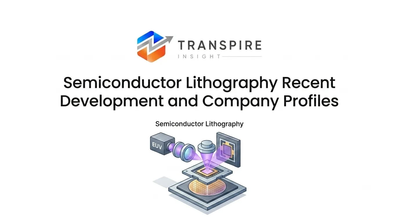
Description
According to a research report published by Transpire Insight, the semiconductor lithography market size is projected to grow from USD 33.45 billion in 2026 to USD 55.63 billion by 2035, at a CAGR of 11.37% during the forecast period 2026-2035. Advanced systems are being pushed by the need for sub-2nm nodes, high-density memory, and 3D chip packaging. At the same time, the next generation of patterning infrastructure is driven by the massive geopolitical foundry expansion and the high performance of AI processors.
Introduction
Currently, the global semiconductor lithography equipment market is growing rapidly and is expected to grow at an unprecedented rate due to the industry's shift to sub-nanometer scaling and high-density complex architecture. With the rise of computing workflows such as generative artificial intelligence and more complex networking designs, precision lithography is increasingly the structural skeleton of semiconductor manufacturing. These exceedingly intricate optical devices can transfer extremely fine circuit designs to silicon wafers using extreme ultraviolet (EUV), deep ultraviolet (DUV), and new alternative printing methods. Thus, lithography platforms are the technology constraints for chip density, power efficiency, and ultimate device performance on a global scale.
Recent Development News
Stay Ahead of Emerging Opportunities with Expert Market Insights by Transpire Insight
Transpire Insight provides comprehensive, data-driven market intelligence to support smarter business decisions. Our research is rooted in comprehensive analysis, authoritative predictions, and industry expertise, enabling organizations to make informed decisions in rapidly evolving markets. In-depth analysis of market segmentation, competitive positioning, regional trends, and emerging investment opportunities in high-growth areas. We blend accuracy with actionable intelligence, empowering companies to uncover new avenues for growth, bolster strategic decision-making, and stay ahead in a dynamic global market.
Semiconductor Lithography Market Size & Statistics
Regional Growth and Demand Analysis by Transpire Insight
Asia Pacific remains the undisputed center of lithography equipment demand, anchored by Taiwan, South Korea, China, and a resurgent Japan. TSMC's continued investment in its Kumamoto facility, combined with Japan's Rapidus initiative targeting 2nm production by 2027 using ASML's High-NA EUV systems, is drawing substantial government backing from Japan's Ministry of Economy, Trade and Industry. China's push for self-sufficiency and Korea's DRAM and NAND expansion at Samsung and SK Hynix further reinforce the region's role as the primary consumer of both DUV and EUV lithography tools, with memory applications emerging as the fastest-growing segment as EUV adoption deepens in advanced DRAM manufacturing.
North America's growth is being driven less by installed base and more by aggressive new capacity additions. Intel's foundry expansion, underpinned by the US CHIPS Act's broader semiconductor funding push, is pulling fresh lithography procurement into the region, with the US lithography equipment market valued at roughly $4.53 billion in 2025. Rising defense, AI, and cloud computing chip demand is compounding this momentum, positioning North America to close the scale gap with Asia Pacific even as the region continues to trail in absolute fab density.
Top 15 Trends in the Semiconductor Lithography Market
High-NA EUV Transition
ASML's High-NA EUV systems are quickly becoming essential for sub-2nm chip production, offering superior resolution over Low-NA tools, with adoption accelerating rapidly across leading foundries.
Advanced Node Scaling Toward 2nm
Leading chipmakers, including TSMC, Samsung, and Rapidus, are racing toward 2nm and 1.4nm production nodes, driving demand for increasingly sophisticated lithography tools and process precision.
DRAM and NAND EUV Adoption
Memory chip manufacturers are rapidly integrating EUV lithography into DRAM production to shrink cell sizes and boost density, making memory the fastest-growing lithography application segment.
Government-Backed Fab Investments
National governments across the US, Japan, India, and Europe are actively funding domestic fabs through generous subsidies, accelerating lithography equipment procurement and reducing import reliance.
Japan's Semiconductor Resurgence
Japan's Rapidus initiative targets 2nm chip production by 2027 using ASML's High-NA EUV technology, backed by TSMC's new Kumamoto fab and substantial METI government subsidies.
Automotive and EV Chip Lithography Demand
Rising semiconductor content in electric vehicles and ADAS systems is steadily boosting demand for lithography equipment serving power, analog, and automotive-grade chip production lines globally.
Top 25 Companies Leading the Semiconductor Lithography Market
1. Merck KGaA (EMD Electronics)
Leading innovator supplying indispensable chemical formulations for modern high-density structural logic nodes.
Founded: 1668 | HQ: Darmstadt, Germany.
Why It Ranks: Globally unparalleled variety of sophisticated photoresists, planarization slurries, and advanced deposition precursors.
Regional Dominance: Massive infrastructure footprints deeply integrated into European and rapidly expanding Asian foundries.
Product Line: Photoresists, developers, advanced cleaning agents, and high-performance organometallic deposition precursors.
2. Shin-Etsu Chemical Co., Ltd.
Global manufacturing leader providing ultra-pure electronic silicon substrates and foundational photolithography materials.
Founded: 1926 | HQ: Tokyo, Japan.
Why It Ranks: Industry-defining purity standards regarding raw materials vital for next-generation EUV lithography.
Regional Dominance: Entrenched supply chain control across critical electronics manufacturing facilities located within Asia.
Product Line: Monocrystalline silicon wafers, Extreme Ultraviolet photoresists, photomask blanks, and encapsulation materials.
3. Air Liquide
Specialized international organization supplying fundamental process gases and custom environmental monitoring infrastructure.
Founded: 1902 | HQ: Paris, France.
Why It Ranks: Unrivaled capability delivering continuously managed, high-volume on-site gas generation for mega-fabs.
Regional Dominance: Widespread distribution networks spanning North American, European, and major Asia-Pacific electronics hubs.
Product Line: Electronic specialty gases, ultra-pure carrier gases, chemical mechanical planarization products, and equipment.
4. The Linde Group
Premier worldwide industrial gases conglomerate engineering specialized chemical delivery infrastructure for fabs.
Founded: 1879 | HQ: Woking, United Kingdom.
Why It Ranks: Pivotal provider of ultra-clean ambient gas technologies essential for sub-10nm fabrication.
Regional Dominance: Exceptional operational resilience across crucial supply networks in the Western hemisphere.
Product Line: High-purity bulk gases, process chemical agents, specialty etching gases, and engineering services.
5. DuPont de Nemours, Inc.
Historic material science pioneer creating specialized polymeric components for intricate multi-layer fabrication.
Founded: 1802 | HQ: Wilmington, Delaware, USA.
Why It Ranks: Advanced research and engineering specialized ancillary products for highly complex advanced packaging technologies.
Regional Dominance: Strongly integrated partnership networks supporting domestic United States foundry expansion initiatives.
Product Line: Advanced photoresists, chemical mechanical planarization pads, specialized lithography cleaners, and dielectrics.
6. Sumitomo Chemical Co., Ltd.
Diversified chemical giant producing vital functional chemicals for advanced microelectronics display sectors.
Founded: 1913 | HQ: Tokyo, Japan.
Why It Ranks: Major chemical contributor facilitating high-performance patterning operations for microscopic integrated architectures.
Regional Dominance: Highly influential market presence throughout extensive East Asian consumer electronics fabrication pipelines.
Product Line: Photoresists, ultra-pure process chemicals, polymer resins, and metallic sputtering target products.
7. Tokyo Ohka Kogyo Co., Ltd. (TOK)
Focused microchemical expert engineered specifically to sustain precision semiconductor patterning processes.
Founded: 1940 | HQ: Kawasaki, Japan.
Why It Ranks: Critical technological breakthroughs regarding formulation optimization for Extreme Ultraviolet exposure methods.
Regional Dominance: Entrenched as the primary chemical resource for major advanced logic foundries in Taiwan.
Product Line: Photoresists, chemical developer solutions, paint removers, and manufacturing auxiliary processing equipment.
8. JSR Corporation
Top-tier electronics materials supplier driving commercial scaling of high-resolution micro-patterning solutions.
Founded: 1957 | HQ: Tokyo, Japan.
Why It Ranks: Direct technical co-development of vital resists with global leading-edge microchip manufacturers.
Regional Dominance: Extensive international operational coverage supporting advanced manufacturing across multiple continents.
Product Line: Advanced EUV photoresists, multi-layer patterning materials, CMP slurries, and cleaning chemistries.
9. BASF SE
Massive multi-national enterprise supplying large-scale customized process chemical formulations globally.
Founded: 1865 | HQ: Ludwigshafen, Germany.
Why It Ranks: Exceptional bulk manufacturing scale paired with rigorous ultra-pure quality control frameworks.
Regional Dominance: Heavily entrenched across traditional European industrial hubs and rapid-growth Asian clusters.
Product Line: Wet processing acids, high-grade organic solvents, planarization mixtures, and custom cleaners.
10. Solvay S.A.
Leading manufacturer providing ultra-resilient fluoropolymers for highly corrosive chemical delivery equipment.
Founded: 1863 | HQ: Brussels, Belgium.
Why It Ranks: Vital supplier ensuring extreme chemical resistance inside ultra-pure wet etching environments.
Regional Dominance: Major component partner for high-purity fluid handling infrastructure engineering groups internationally.
Product Line: High-performance fluoropolymers, cleaning peroxides, wafer etching compounds, and chemical mechanical agents.
Conclusion
The semiconductor lithography and allied chemicals markets remain the absolute baseline for global technology progression. As technical nodes contract and processing complexities escalate, the interdependency between next-generation optical equipment makers and high-purity chemical formulators will grow exponentially. Driven by escalating artificial intelligence infrastructure needs and regional supply diversification mandates, market leaders will continuously direct heavy capital allocations toward extreme ultraviolet innovation and sustainable chemical alternatives. Ultimately, this ecosystem will dictate the baseline efficiency and structural reality of the world's next computational era.


Send us a brief description of your challenge and we'll get back to you within 24 hours.

 inquiry@transpireinsight.com
 APAC:+91 7666513636
 Address


